
Measurements
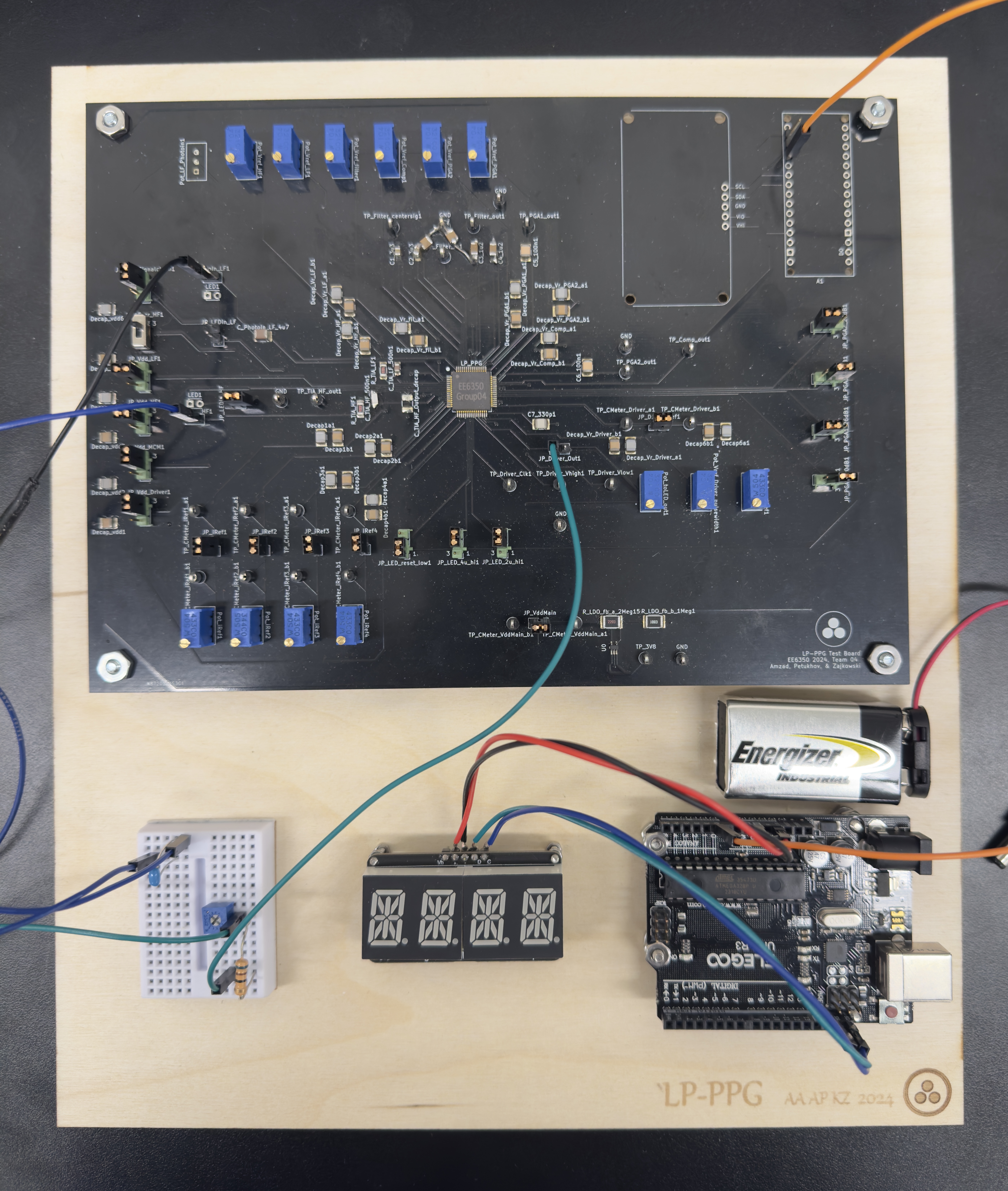
Figure 1. Testbench Setup
The figure above shows the testbench that was used to take measurements from the chip. The top of the testbench features the PCB with the chip in the center. On the bottom left of the testbench is a breadboard used to bias the IR LED and photodiode receiver. In the middle is an alphanumeric display, used to display a person's heart rate in BPM. To the right of the display is the Arduino that receives the comparator's output to perform digital signal processing to extract a heart rate, which is transmitted to the alphanumeric display via I2C. The Arduino is powered by the 9V battery above it. While the Arduino and display were initially intended to be fixed to the PCB, an accident with the Arduino Nano late in testing necessitated the switch to an Uno as a backup, so a wider mounting platform was laser-cut and assembled to accommodate the larger hardware.
Power Measurements
| Block | Current (uA) | Power (uW) |
|---|---|---|
| TIA (LF) | 219 | 547.5 |
| TIA (HF) | 226 | 565 |
| Mixer | 162 | 405 |
| Filter | 961 | 2402.5 |
| PGA1, PGA2, Comparator | 156 | 390 |
| Master Current Mirror | 109 | 272.5 |
| Total AFE (Calculated) | 1724 | 4310 |
| Total AFE (Measured) | 1776 | 4440 |
| Total AFE (Simulations) | 1723 | 4307.5 |
| LED Driver Static Elements (Measured) | 133 | 332.5 |
| LED Driver Static Elements (Simulations) | 112 | 280 |
To measure the static power consumption of individual blocks, a combination of turning off power domains via jumpers and bias currents on the Master Current Mirror were used. The only set of blocks that could not be evaluated individually for power measurements were PGA1, PGA2, and the Comparator. From the power measurements shown above, the measured chip power consumption was similar to the power simulations of the chip with an additional 140uW of power being consumed. The LED Driver static element power measurements were also shown to be roughly in line with the simulation results when the LED Driver Inverter was off. The additional current consumption of the chip is due to the LDO producing a slightly higher VDD from the biasing resistors being a bit off in resistance. Overall, these measurements show that the chip was able to achieve the 5mW power budget specified for the Analog Front-End.
LED Driver Signal
Initially powering on the LED Driver showed a high amount of jitter on the clock frequency from the SR Latch. The duty cycle of the LED output voltage also showed a very non-linear response for a linear change in V_pw, where the duty cycle would jump from 7% to 50%. From debugging the circuit, it was found that the on-chip resistor bridge used to create the two reference voltages, V_Low and V_High, would collapse due to the high current draw of the LED driver inverter. Adding two capacitors to stabilize those reference voltages allowed the LED Driver to have a very linear response between V_pw and duty cycle.
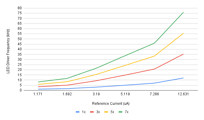
Figure 2. LED Driver Frequency for each Current Mode
The LED Driver was characterized to measure the output frequency of the oscillator for the reference current being sent to the current mirror for each current mode (1x, 3x, 5x, 7x). Sweeping the reference current showed a linear relationship between the reference current and output frequency. However, as the LED Driver approached higher frequencies, the relationship between current and frequency began to deviate, where more current did not translate to higher frequency. Measurements of the SR Latch clock, which feeds is used by the Mixer, showed that the clock's duty cycle was between 48.7% and 52.4% for the frequency range of the LED Driver. This relationship showed that the SR Latch clock's duty cycle would decrease towards higher frequencies. This deviation in duty cycle of the SR Latch clock was due to a small mismatch between the PMOS and NMOS in the current mirrors.
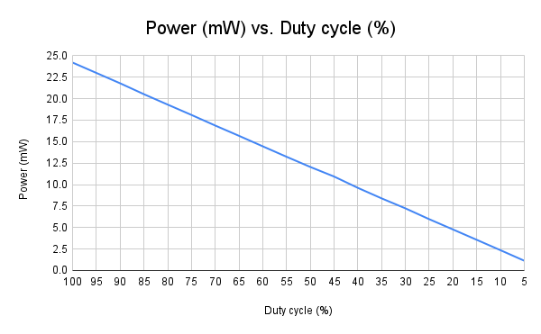
Figure 3. LED Driver Power Consumption with Respect to Duty Cycle
The graph above shows the power being supplied to an LED as a function of duty cycle. In this setup, a 100Ω resistor was placed in series with the IR LED that was chosen to be used to measure heart rate. As shown by the graph, the LED Driver's power linearly decreases with respect to a smaller duty cycle, where at a minimum of 5% duty cycle, the power is 1.1mW.
Analog Front-End Signal Chain
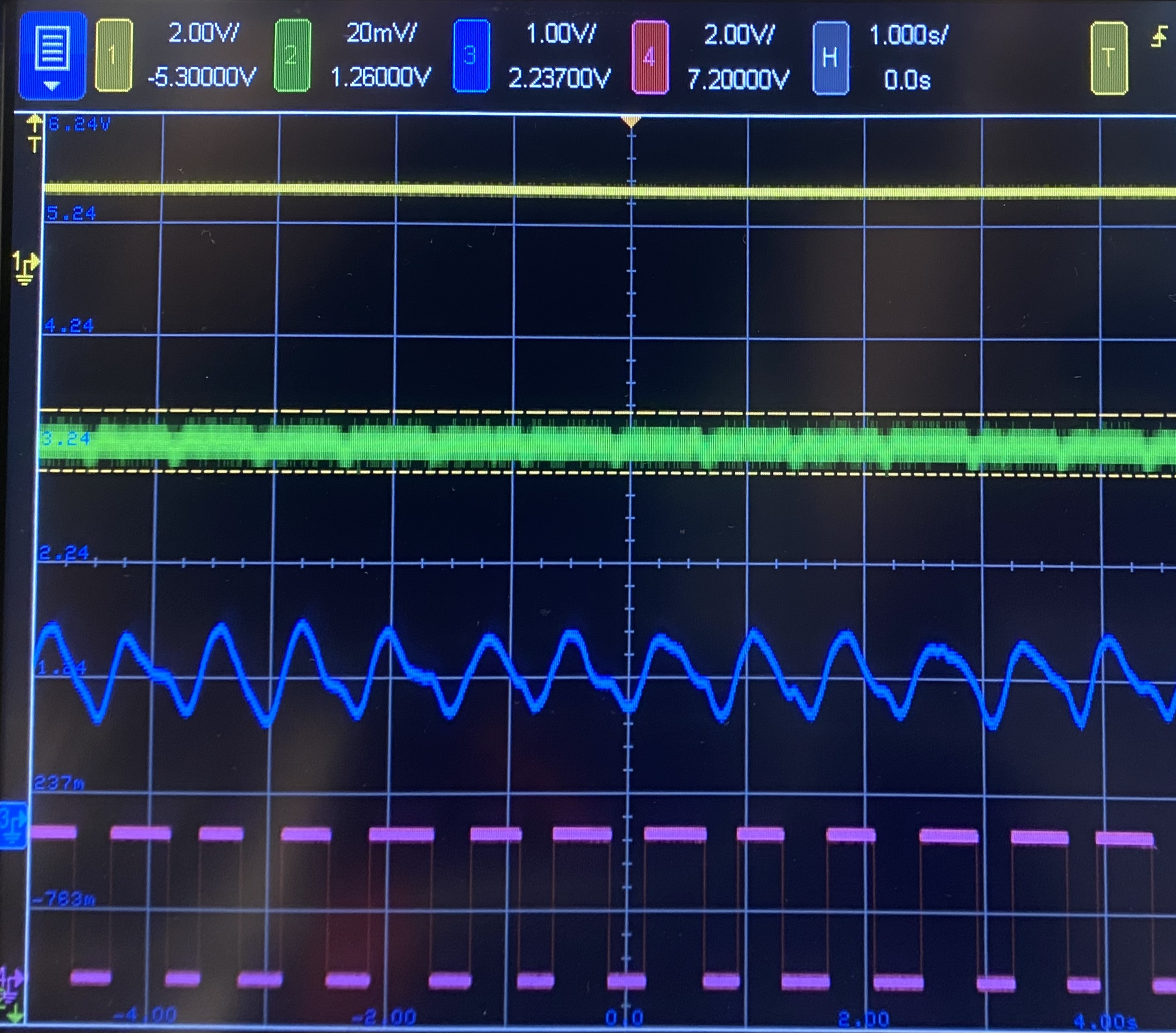
Figure 4. Signal In, Signal Out, LF Chain - Signal to LED (Yellow), Signal from TIA (Green), Analog Out (Blue), Digital Out (Pink)
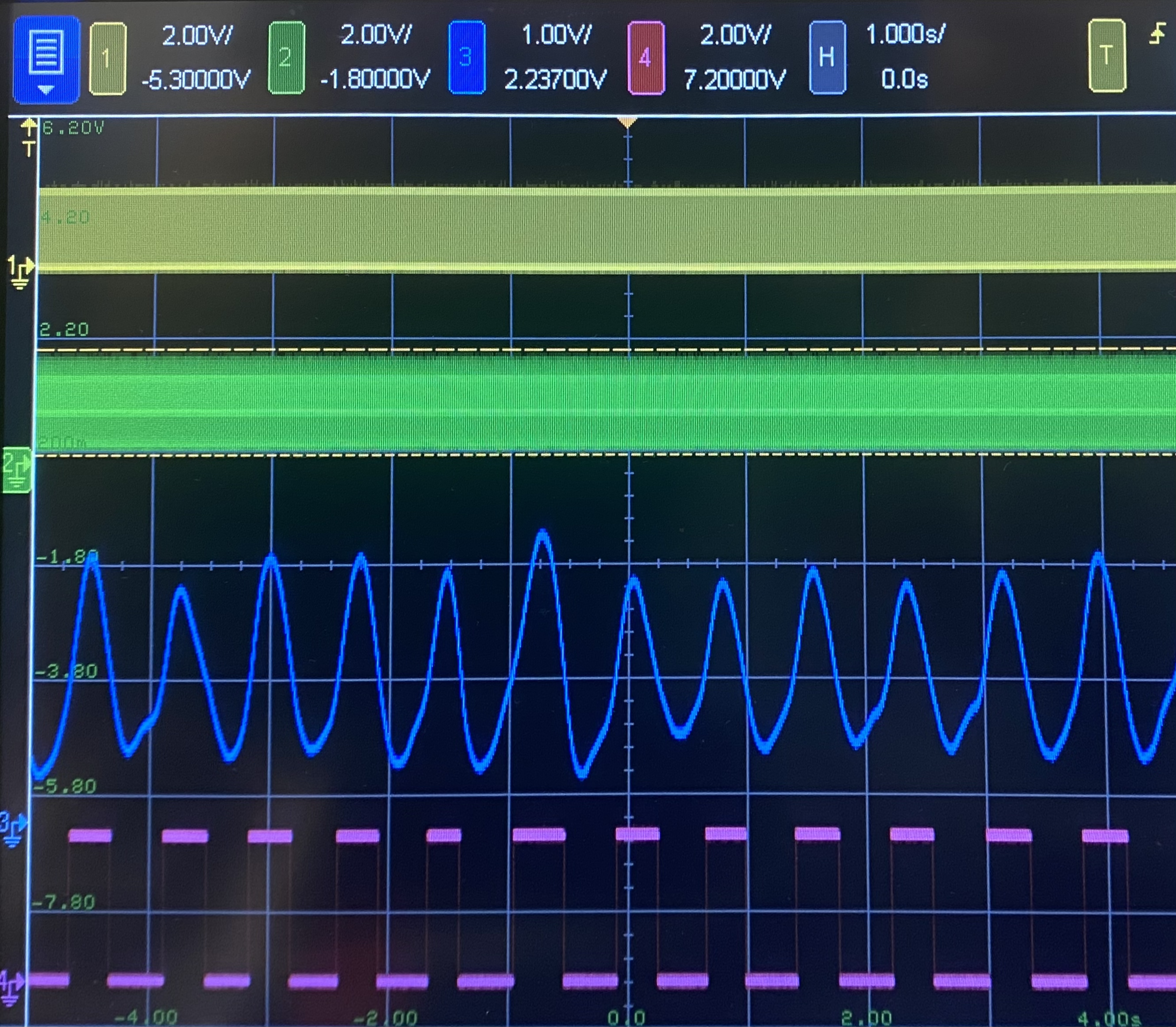
Figure 5. Signal In, Signal Out, HF Chain - Signal to LED (Yellow), Signal from TIA (Green), Analog Out (Blue), Digital Out (Pink)
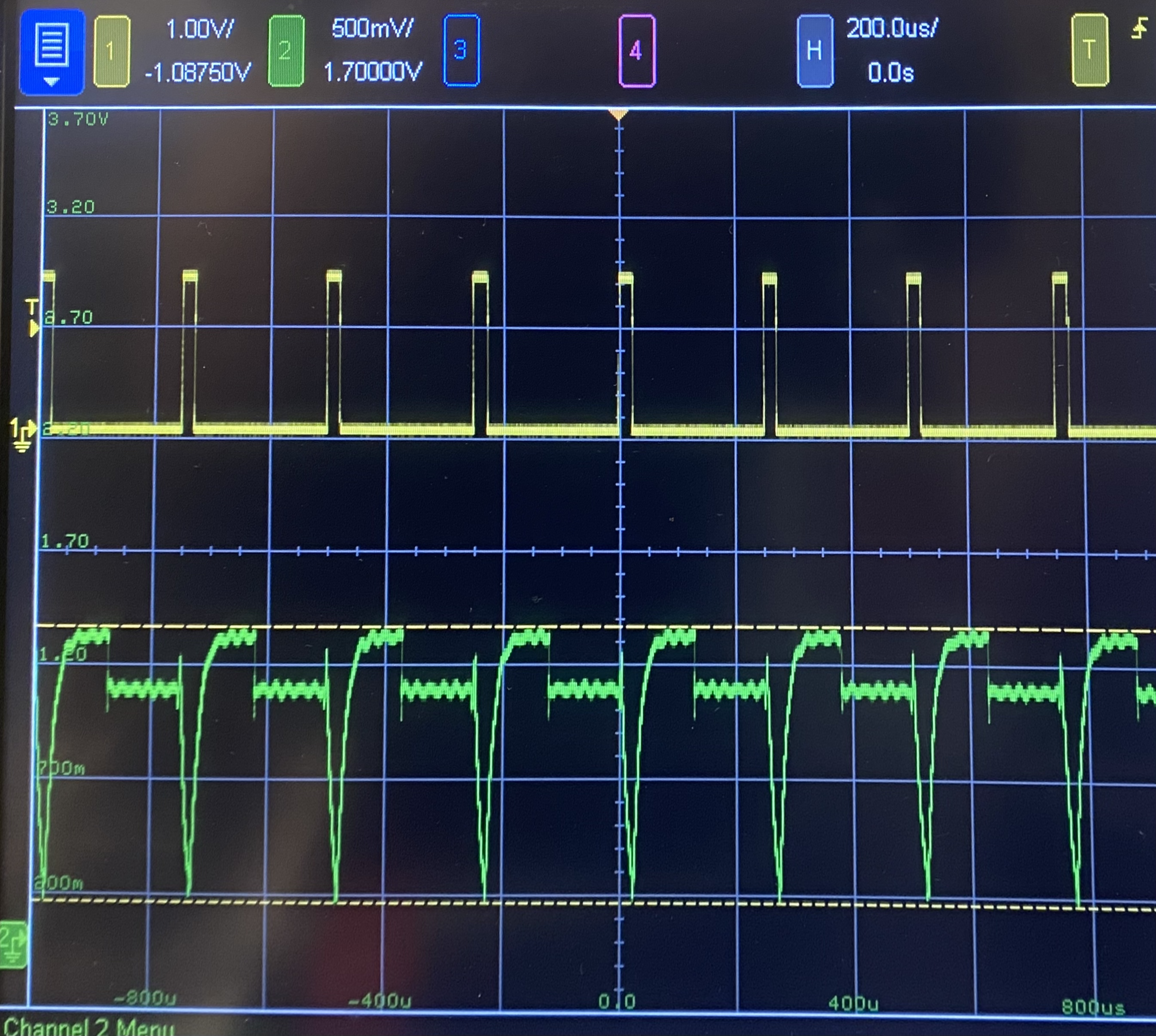
Figure 6. High-frequency Signals: HF Chain - Signal to LED (Yellow), Signal from TIA (Green)
In the LF chain, the signal sent to the LED can be varied from a 100% to 5% duty-cycled square wave. This signal is transmitted reflectively to the user's finger and the photocurrent is passed through a DC-blocking capacitor and amplified by the LF TIA. The resultant signal, in green, is fed into the bandpass filter to remove low- and high-frequency components outside of the desired passband and then amplified by two PGAs (6.66x/10x/20x variable gain) before being converted to a 2.5V binary signal by the comparator. This digital signal encodes the beat-to-beat interval in its rising edge, as this corresponds to the time of expansion of the finger's capillaries with the heart-beat's pressure wave.
In the HF chain, the LED is duty cycled to a percentage below 30%, and is then transmitted to the user, received by a broadband TIA, and fed into a mixer - the signal now contains a mix of frequency components <10kHz, including a downmixed 1Hz signal of interest. When this is fed into the bandpass filter, the up-mixed high-frequency components are removed alongside the bulk of the original 1/f spectral noise, and the down-mixed the 1Hz output component is boosted & converted to a digital signal as before.
Duty Cycle vs SNR, LF vs HF
In the following gallery, FFT captures of the analog output from each signal chain are shown. For all measurements, a current of 20mA was fed to the LED in the transceiver, limited by a series resistor, with the driver clock running at f_clk = 4kHz. A clear visual representation of signal strength vs duty-cycle for each chain can be qualitatively observed for each chain, and the following tables summarize measurements from the captures. Below the images, further discussion will be given understanding the observed behaviors, and a methodology for estimating SNR from these measurements will be discussed, applied, and plotted.
| Duty Cycle [%] | Signal Strength [dBV] | Avg Noise-Floor (passband) [dBV] |
|---|---|---|
| 100 | -25.3 | -50 |
| 70 | -29.6 | -50 |
| 50 | -31.8 | -50 |
| 35 | -33.5 | -50 |
| 25 | <-34.4/td> | -50 |
| 10 | -36.0 | -50 |
| 5 | -39.4 | -50 |
| Duty Cycle [%] | Signal Strength [dBV] | Avg Noise-Floor (passband) [dBV] |
|---|---|---|
| >30 | N/A | N/A |
| 25 | -19.4 | -53 |
| 20 | -19.1 | -53 |
| 15 | -16.9 | -53 |
| 10 | -20.8 | -53 |
| 5 | -28.4 | -53 |
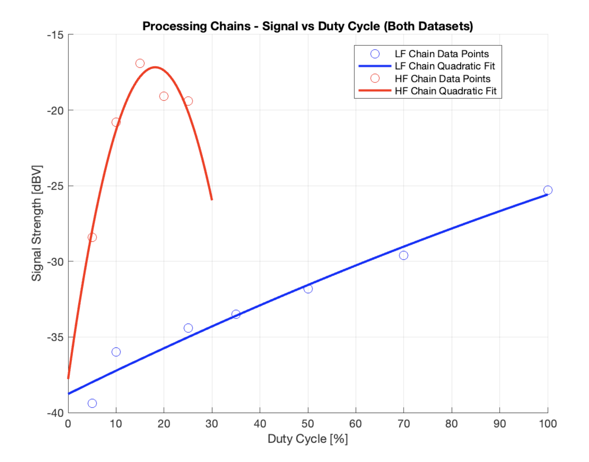
Figure 7. Extracted Signal vs LED Duty Cycle
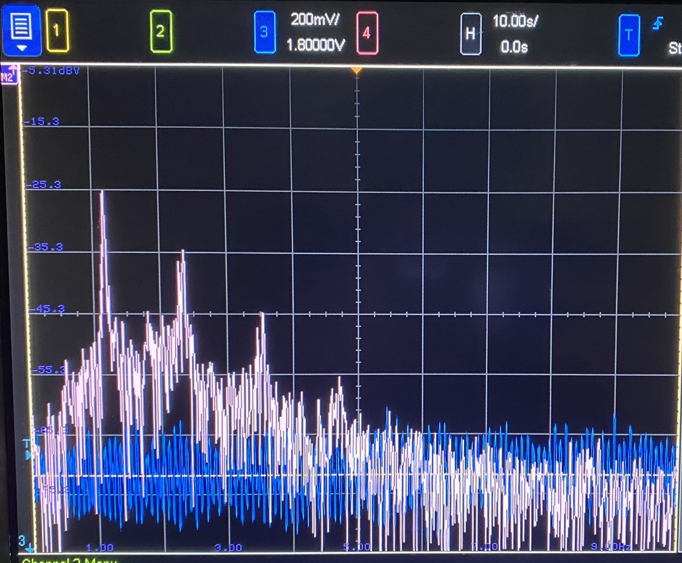
Figure 8. LF - 100% Duty Cycle - FFT, real user, 100 seconds
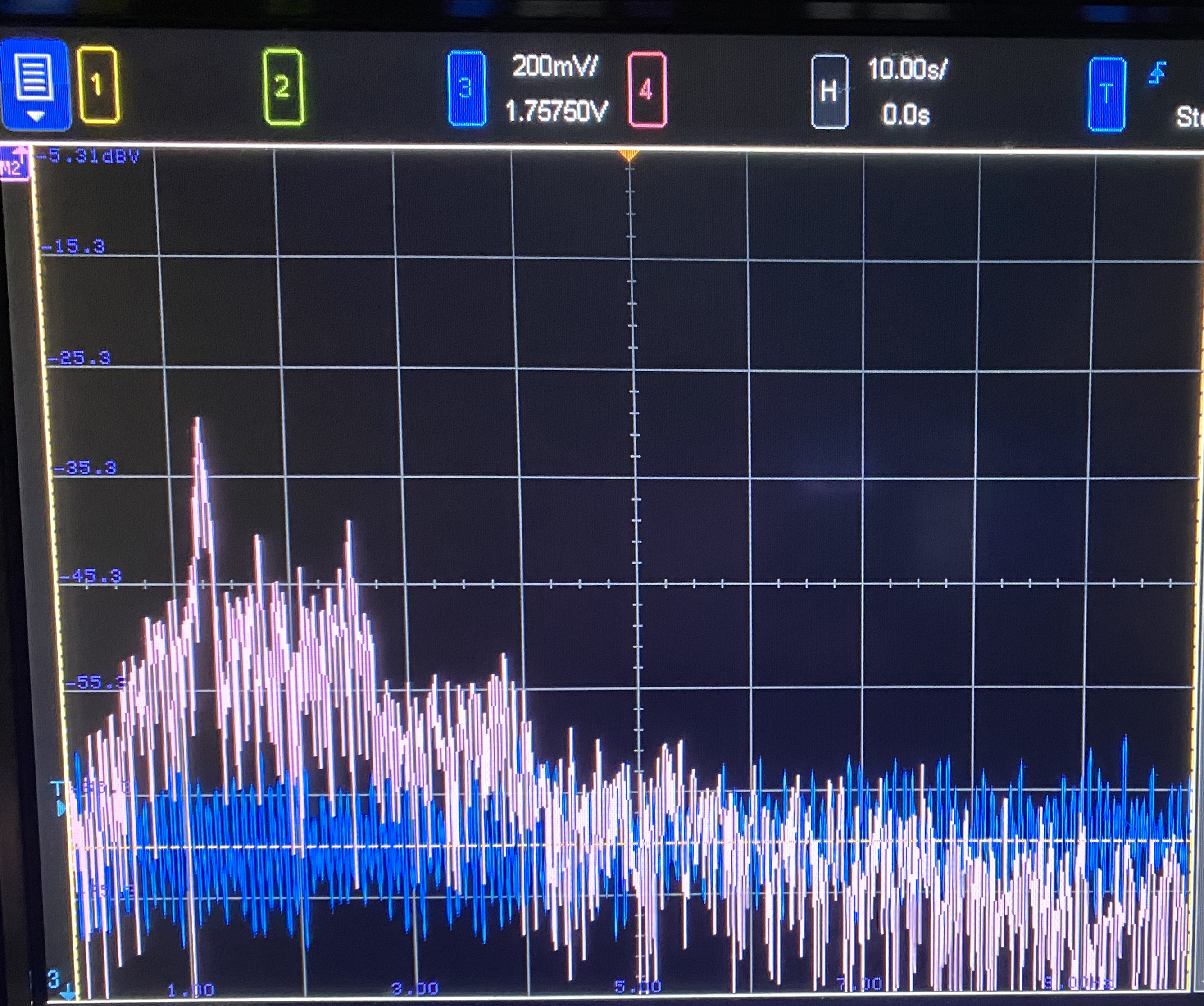
Figure 9. LF - 70% Duty Cycle - FFT, real user, 100 seconds
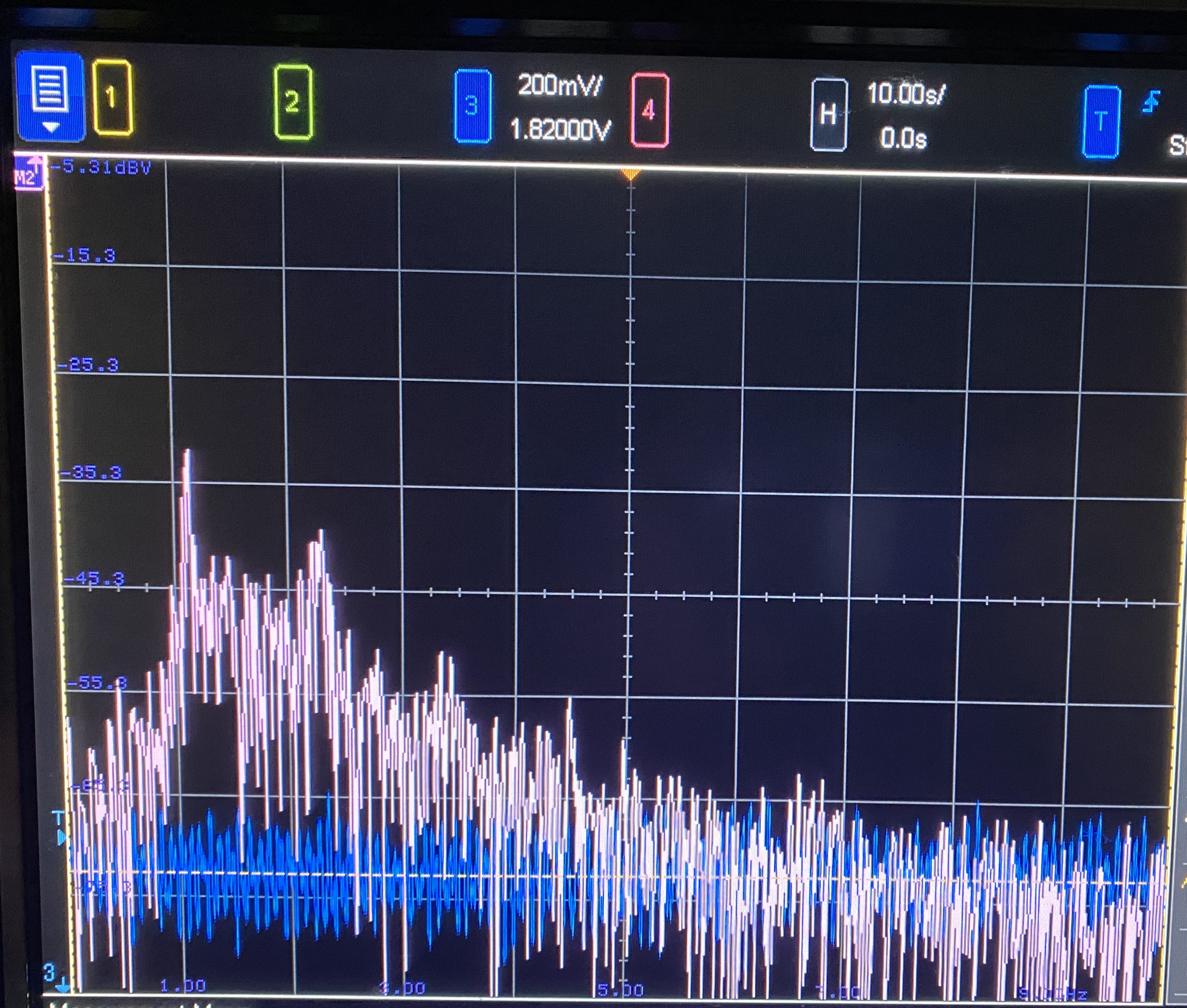
Figure 10. LF - 50% Duty Cycle - FFT, real user, 100 seconds
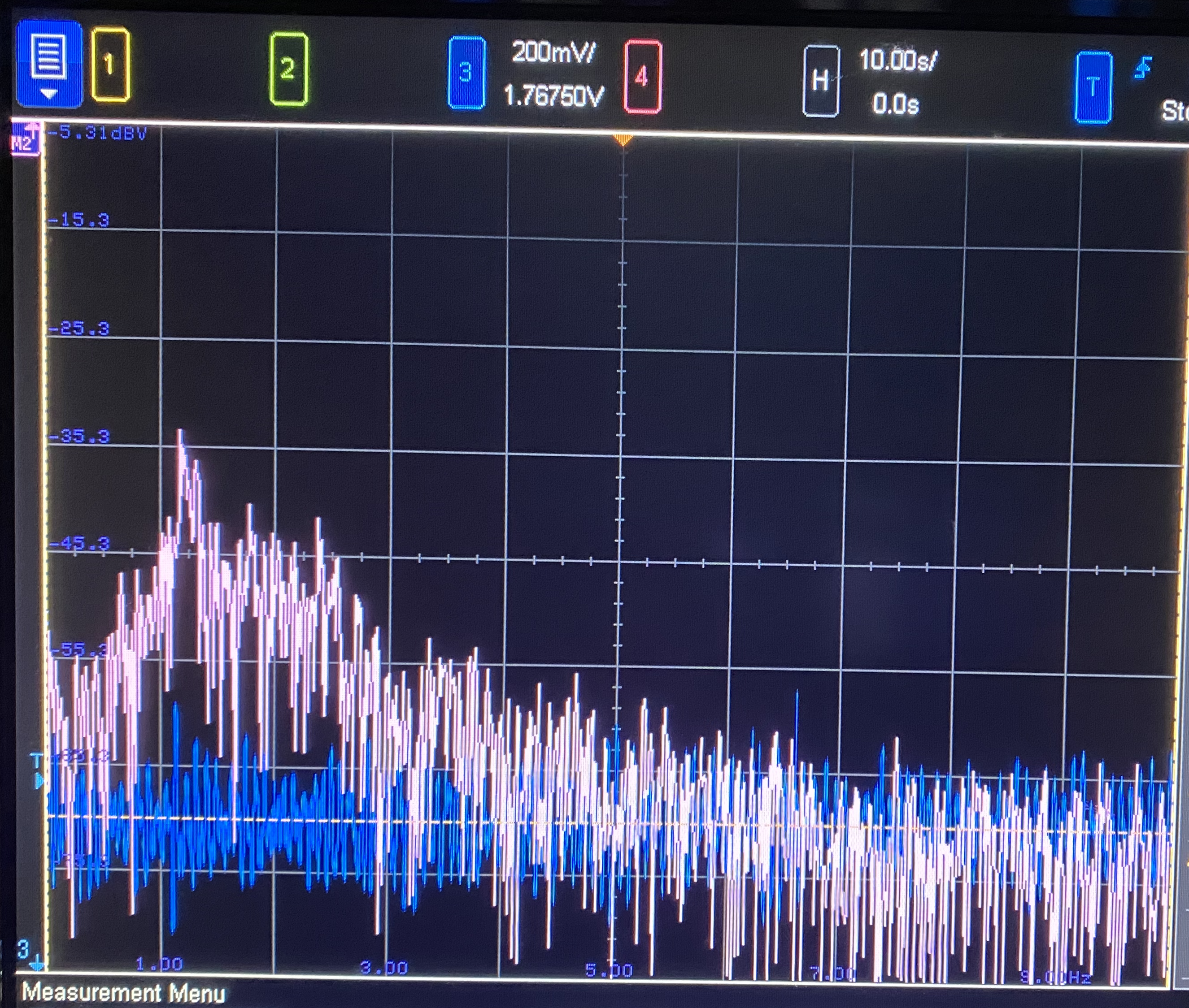
Figure 11. LF - 35% Duty Cycle - FFT, real user, 100 seconds
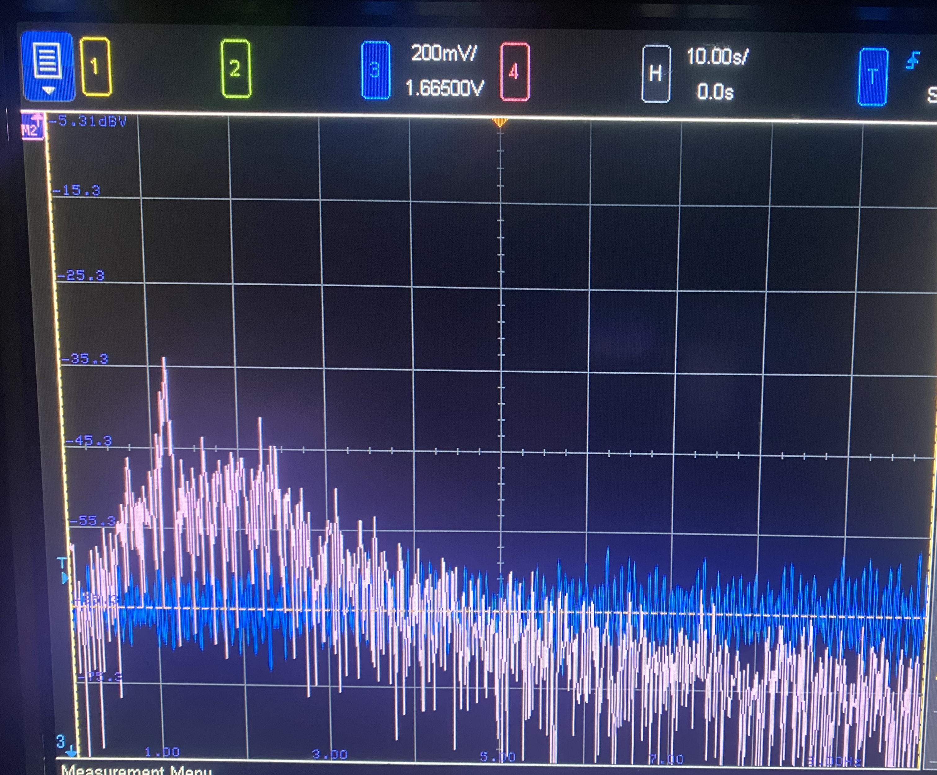
Figure 12. LF - 25% Duty Cycle - FFT, real user, 100 seconds
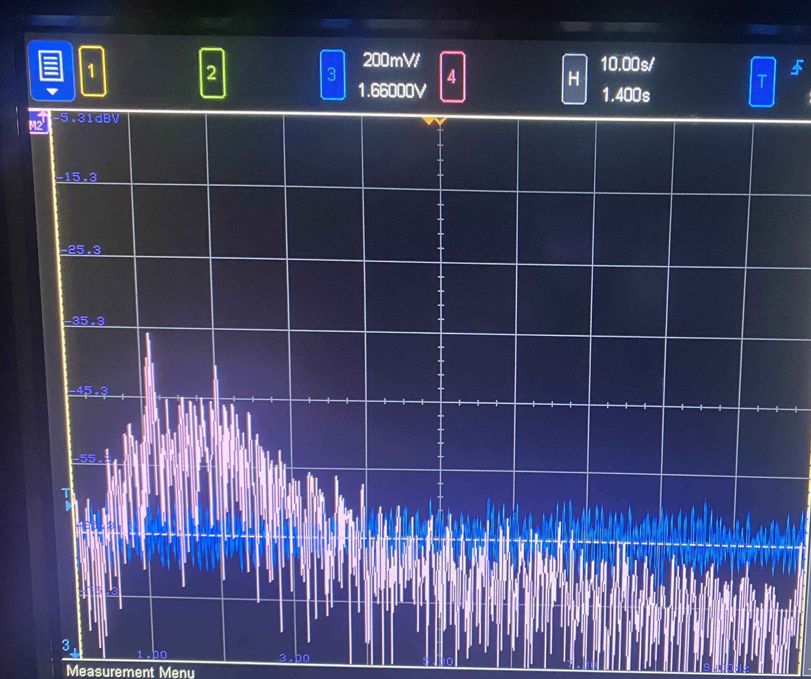
Figure 13. LF - 10% Duty Cycle - FFT, real user, 100 seconds
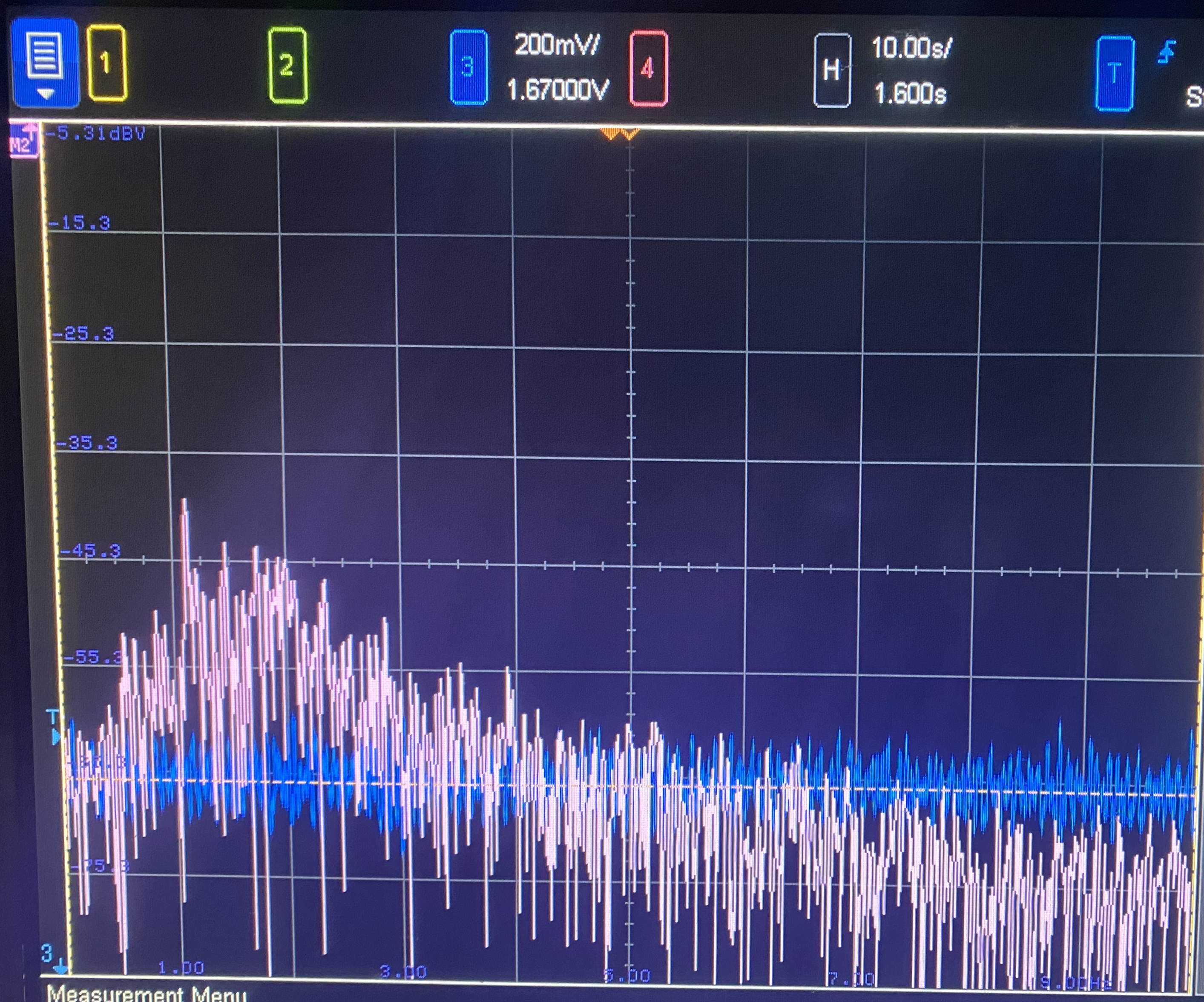
Figure 14. LF - 5% Duty Cycle - FFT, real user, 100 seconds
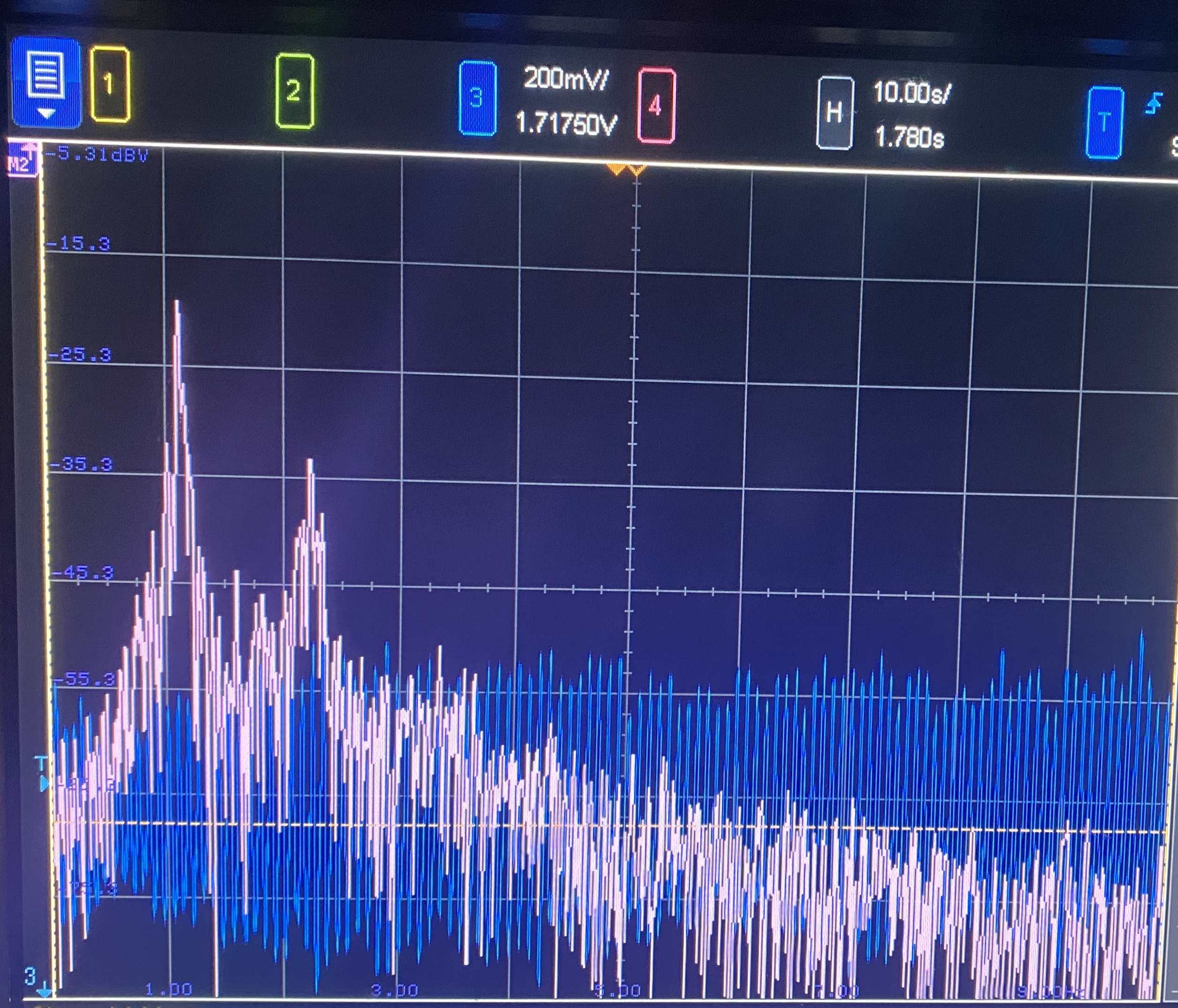
Figure 15. HF - 25% Duty Cycle - FFT, real user, 100 seconds
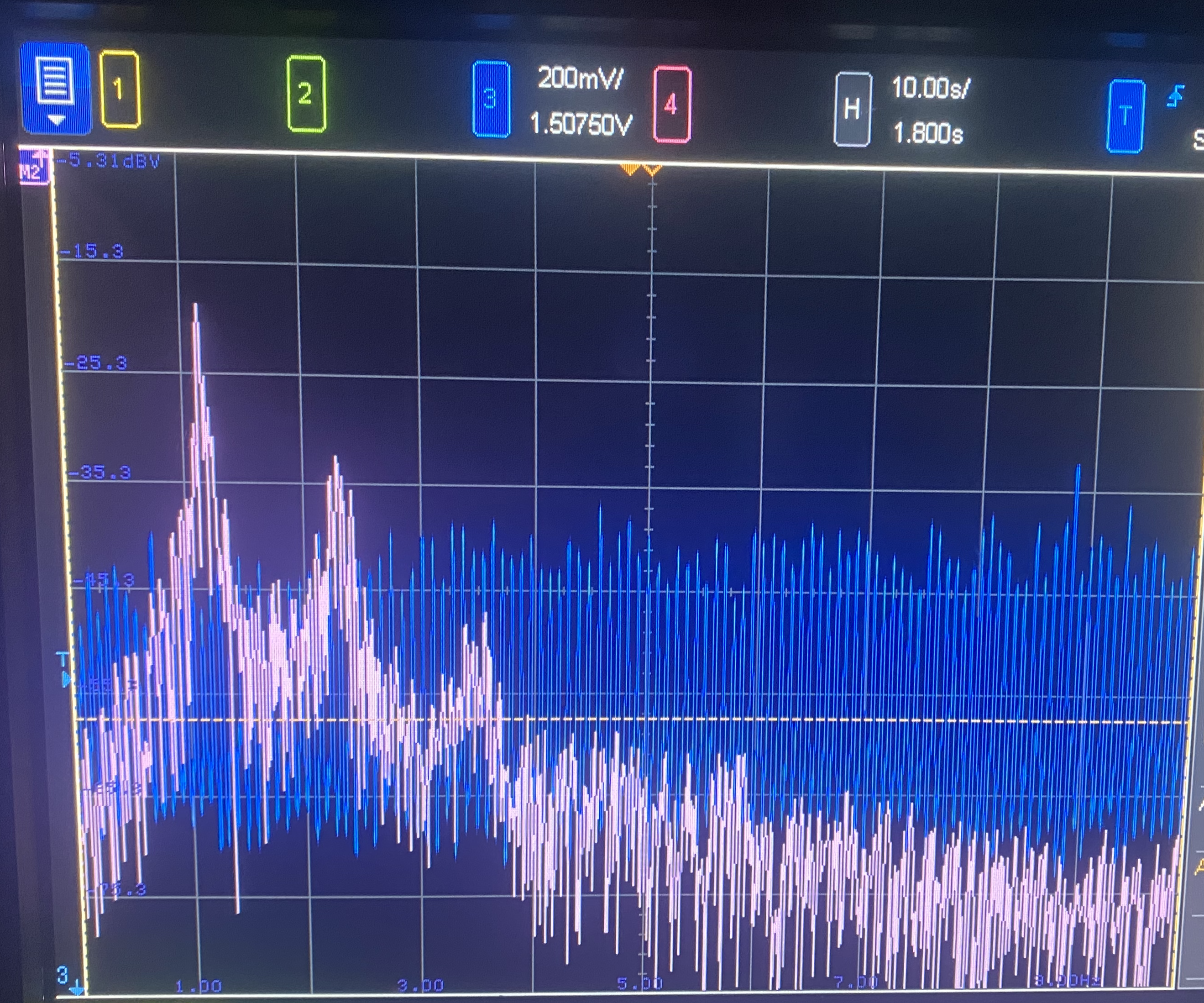
Figure 16. HF - 20% Duty Cycle - FFT, real user, 100 seconds
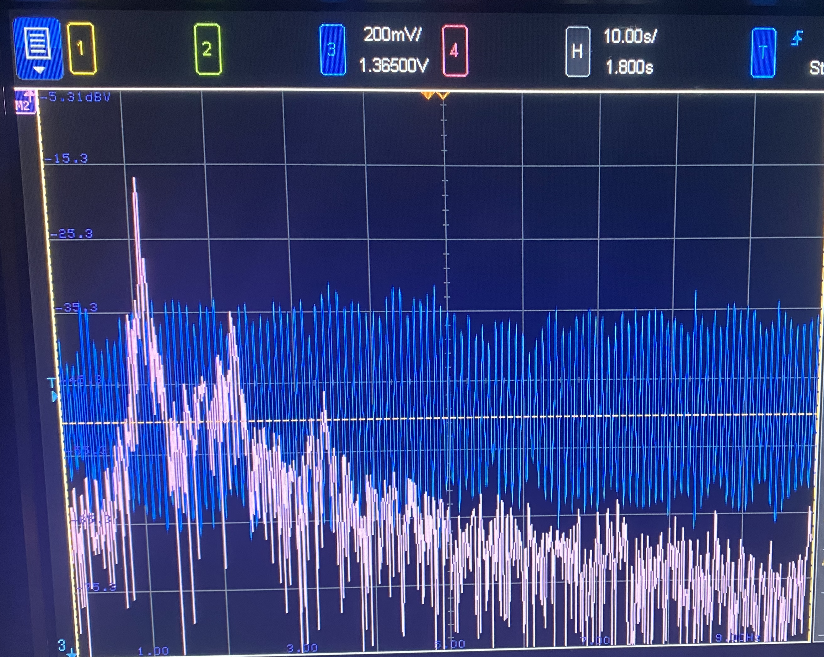
Figure 17. HF - 15% Duty Cycle - FFT, real user, 100 seconds
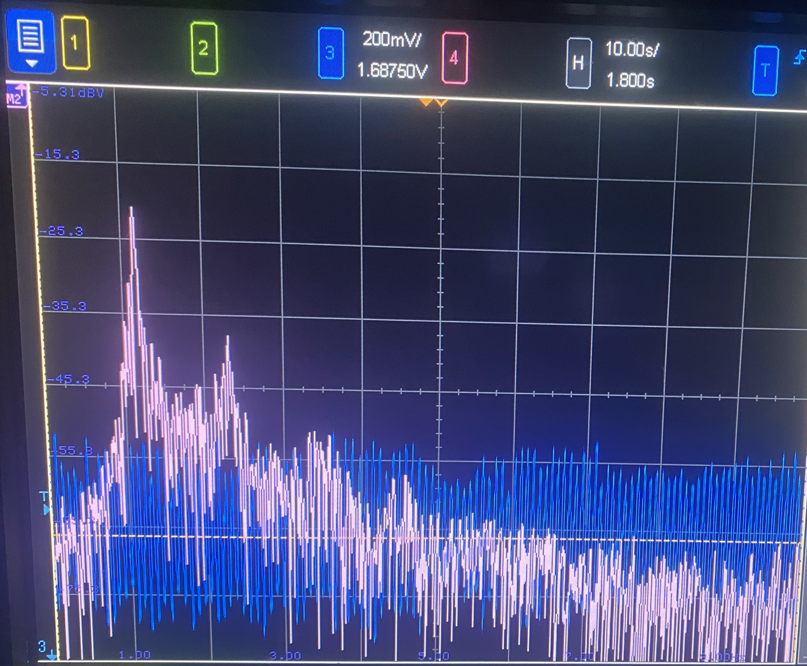
Figure 18. HF - 10% Duty Cycle - FFT, real user, 100 seconds
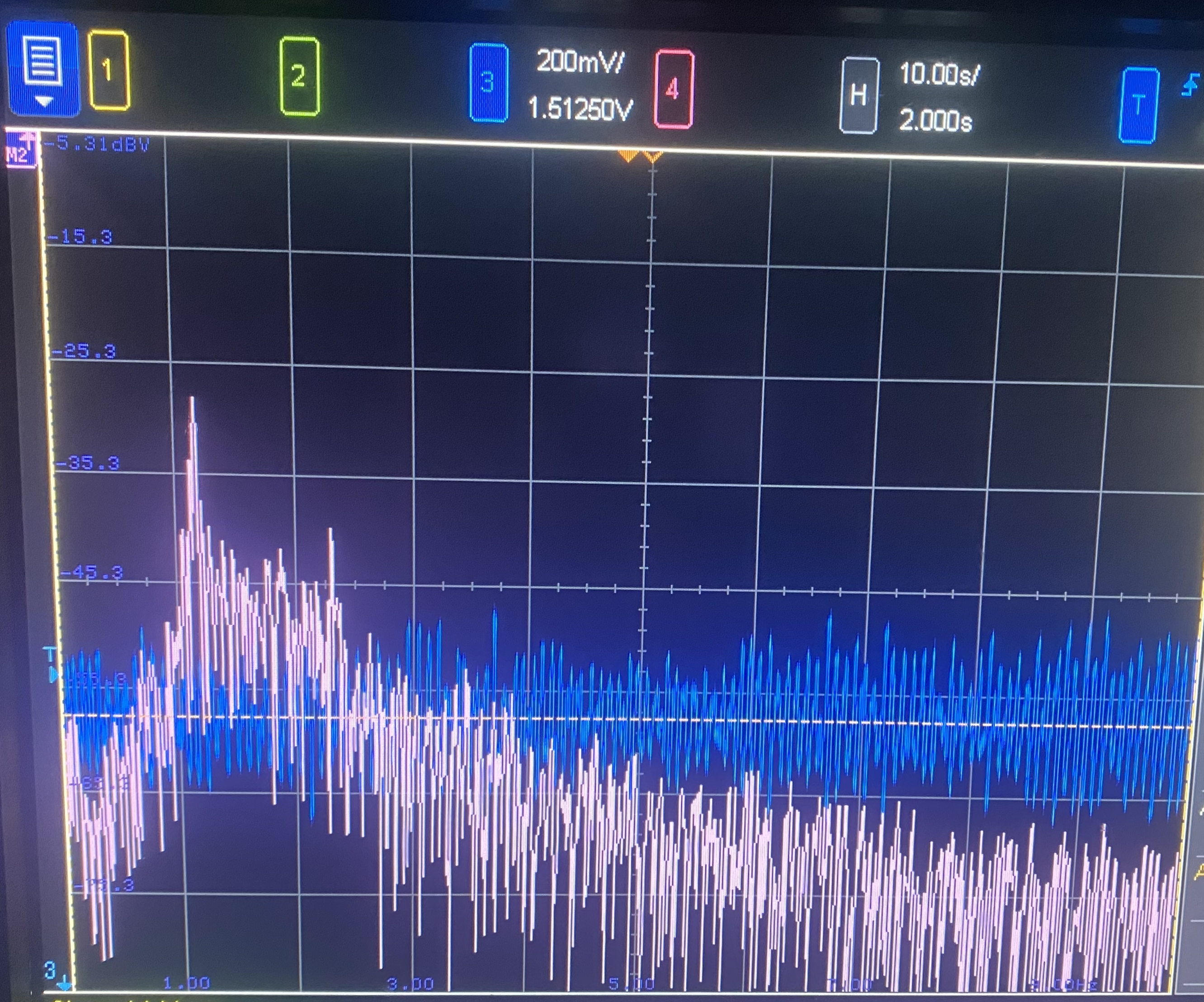
Figure 19. HF - 5% Duty Cycle - FFT, real user, 100 seconds
As seen, the baseline LF chain produces a roughly linear relation between duty cycle and received signal strength - to be precise, the fit for signal strength is logarithmic in the above logarithmic plot, indicating underlying linearity. Although a precise statement of total signal power would require integrating the 3 signal peaks in each plot and subtracting the surrounding noise-floor (e.g. some measurements show narrower or wider ‘delta's in their FFTs, indicating variance in the user's heart rate during the ~2 minute recordings). Regardless, the fundamental FFT peak of each plot provides a first-order understanding of how SNR tracks in each case.
For the LF chain, it can be seen that 70% DC is approximately 4dB below 100% with the expectation being a -3.1dB difference in a perfectly linear relationship, and the 50% measurements are approximately -7dB below 100%, with the expectation being -6dB. For the HF chain, it was observed that the recovered signal strength has no clear correlation for most of the valid signal range except that its performance drops off below 10% d.c. and above 25% d.c.. The performance fall-off below 10% duty-cycle is a result of the slight mismatch in delay/synchronization between the signal entering the mixer and the clock signal generated on-chip. This synchronization issue could have been corrected if there had been a manual control mechanism to delay the on-chip clock sent to the mixer, but due to limits in I/O pins during design, such a control was not implemented. At higher duty cycles, the output of the mixer begins to compress, and the down-mixed 1Hz component very rapidly is killed by the higher-frequency components such that this chain does not operate above ~30% duty cycle. Decreasing the amplitude of current sent to the LED reduces all signal amplitudes and increases the range of duty cycles over which the mixer / HF chain can operate, but in practice this would not be helpful - the signal of interest would be attenuated linearly alongside the unwanted signal components, and since the point of this signal-chain is to enable operation at lower duty-cycles, no system-wide benefit would be achieved by this.
Ultimately, even ignoring the average drop in the observed noise-floor at the output of the HF chain, the signal recovered by the HF chain significantly outperforms the baseline LF chain. At a first glance, even at its worst performance (5% d.c., when the LED begins consuming less power than the rest of the chip and system-power is <10mW in total) it outperforms all LF chain operating conditions except 100% duty cycle. If the ~5dBV difference in noise-floor heights is accounted for, the HF chain always outperforms the LF chain in its valid operating range.
Producing a specific statement of SNR is difficult from the saved captures, but by linearizing the noise-floor within the passband as a window from 0.8-2.4Hz and approximating the received HR signals, using just the fundamental peak, as isosceles triangles with some height peak signal, [dBV] and width [BW where signal > noise-floor window], the following estimations of SNR can be attained.
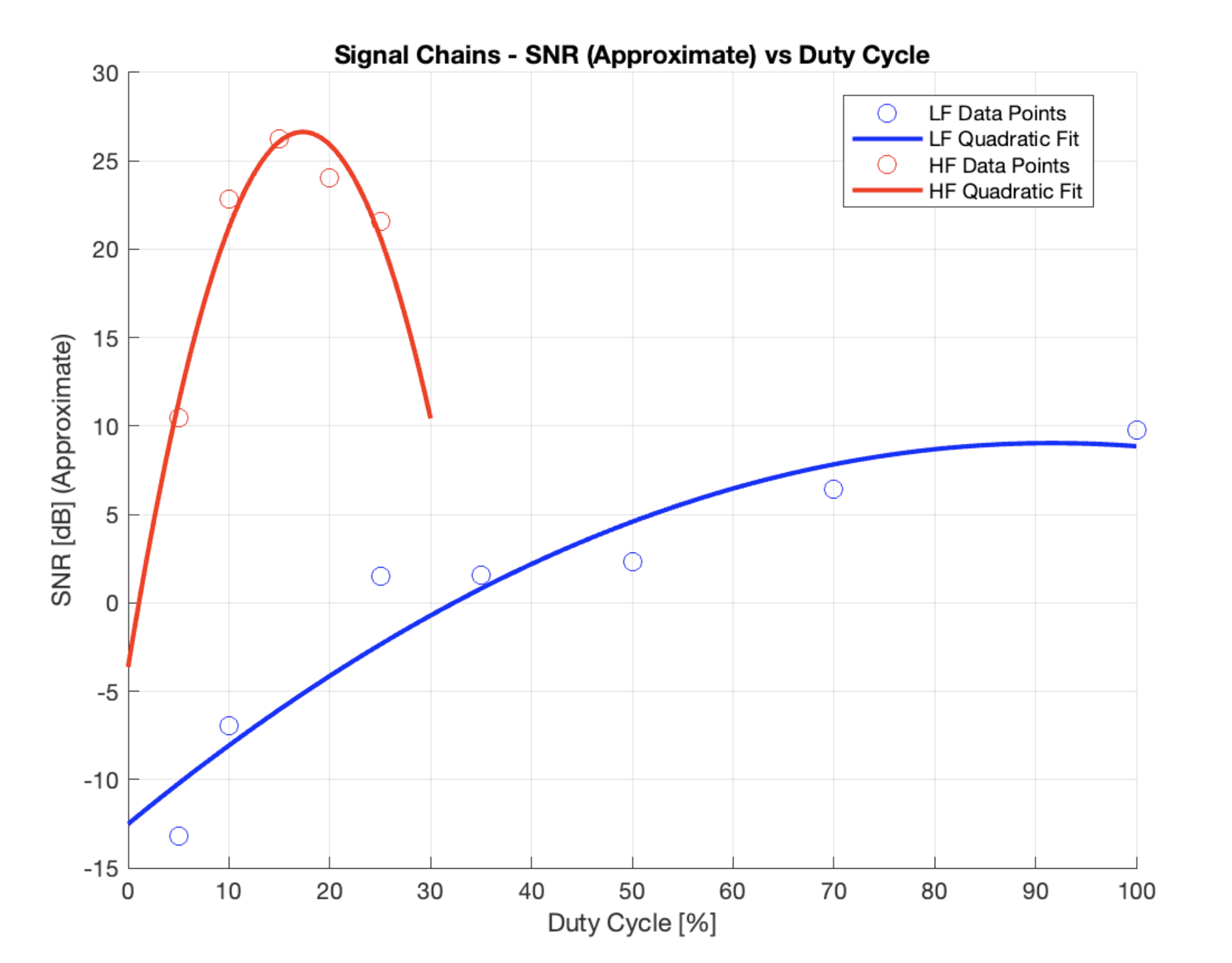
Figure 20. SNR vs Duty Cycle by Signal Chain
While this form of geometric approximation is not perfectly accurate, it does partially compensate for the variance in user heart-rate between different recording sessions, which spreads signal power out from the center frequency. The resultant approximate SNR plots show similar trends as the original data, but with the logarithmic relationship between the LF chain and duty cycle more clearly visible. Note that SNR at all points could be improved by supplying more current intensity to the LED (e.g. up from 20mA max to the emitter's rated maximum of 100mA, which the chip can supply), but these are the moderate power levels that were chosen to demonstrate the system.
The design target was to create a system that maintained >10dB of SNR in its extracted signal, and this plot shows that the chip was able to achieve this goal. The extent to which the HF chain outperforms the LF baseline (even without full phase-control at the inputs of the lock-in amplifier) demonstrates the clear advantages of extracting the higher-amplitude and reduced-1/f signal components from duty-cycled optically interrogated biosignals.
Accuracy Comparison between the Chip and a Commercial Option
A detailed comparison of reliability of the LP-PPG chip versus an off-the-shelf benchmark was not performed for the full sweep of duty cycles and LED currents achievable with this system. However, early on in testing, it was confirmed that the rising-edge interval of encoding heart rate was viable. Seen below, a brief FFT of the chip's digital output compared live against an off-the-shelf PPG system. The principle frequency of the recovered square wave over 10 cycles is 1.22Hz, or 73.2 BPM. As shown, this is also the recovered signal from the purchased system, shown reading 73 BPM.
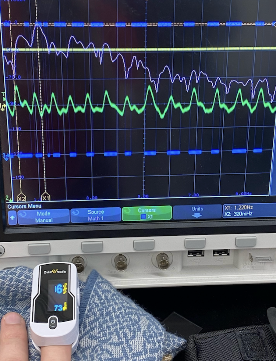
Figure 21. Comparing Chip's Performance to Commercial Sensors
Experimentally, it was found that by averaging a queue of 10 past samples on the testing system's Arduino, the system would jitter/update more quickly than the commercial solution, but as the user's heart-rate always settled to the same value across both systems given 30 seconds or so without major movements. It is believed that the off-the-shelf solution likely averages over a long period and/or applies more selective reading error-correction than the implemented DSP on the Arduino, though the off-the-shelf PPG's analog output traces aligned indistinguishably.