PCB Design
To complete the whole system and verify the chip' s functionality, we designed a 2-layer PCB using KICAD. The schematics are shown in Figure 1
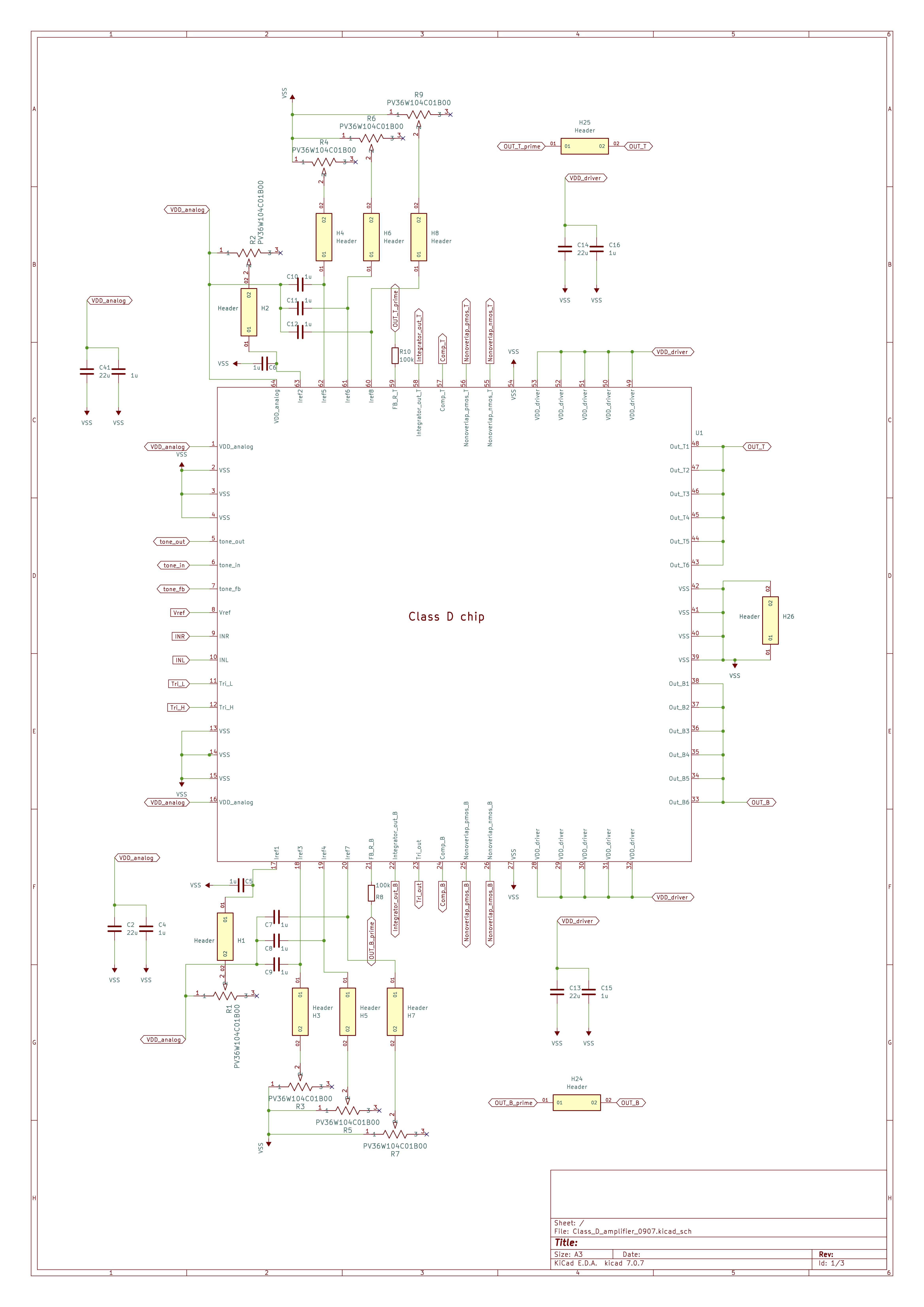

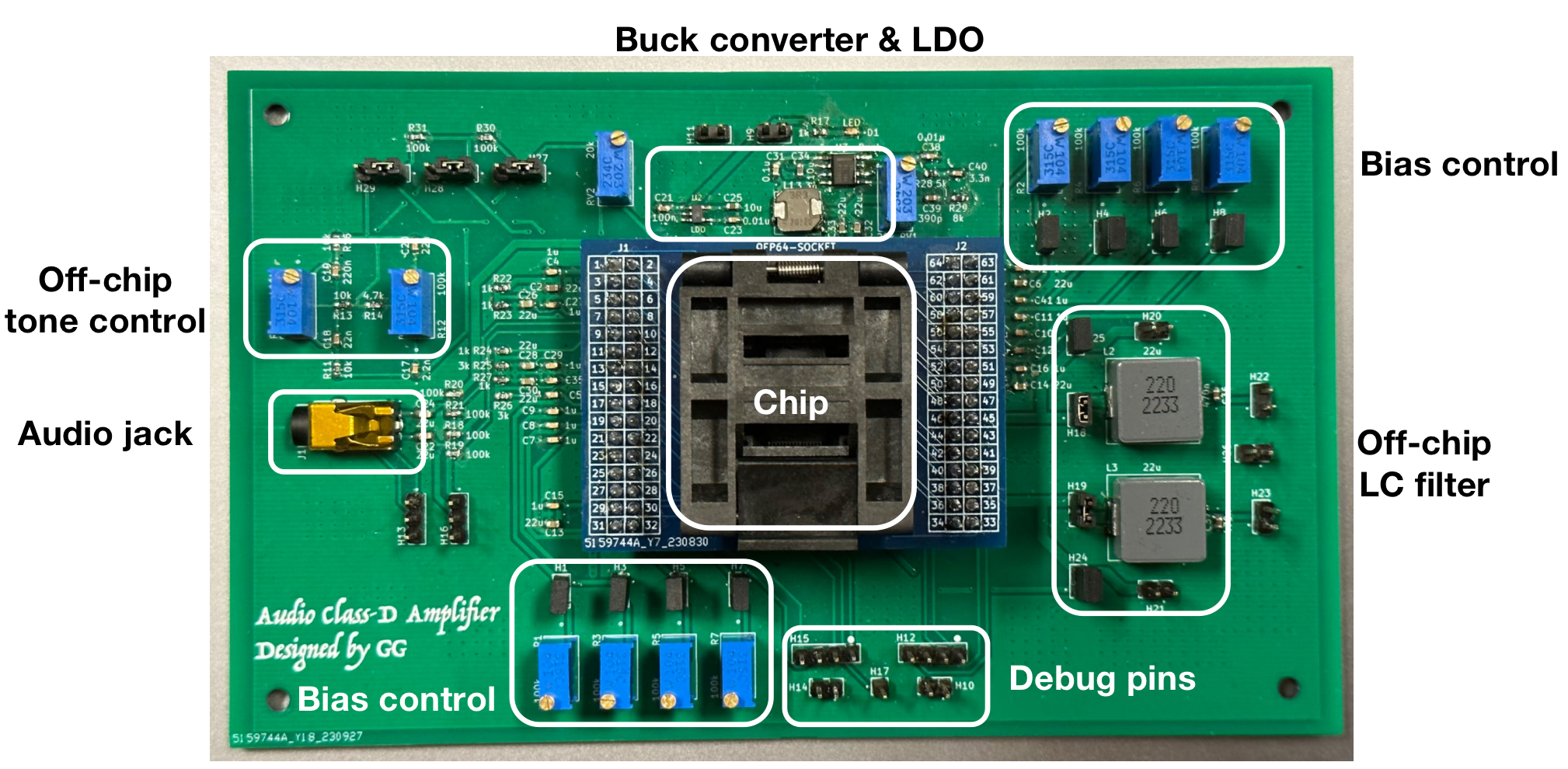
As shown in Figure 1. a, we used multiple potentiometers to adjust the reference currents, which allowed us to adjust the triangle wave frequency, dead time, and OTA reference currents.
As depicted in Figure 1. b, we used LDO to provide the power supply for VDD_analog and Buck for VDD_driver. The 3.5mm audio jack is used to input the audio signal, and an LC filter is used to filter out the high frequencies to obtain a clear audio sound.
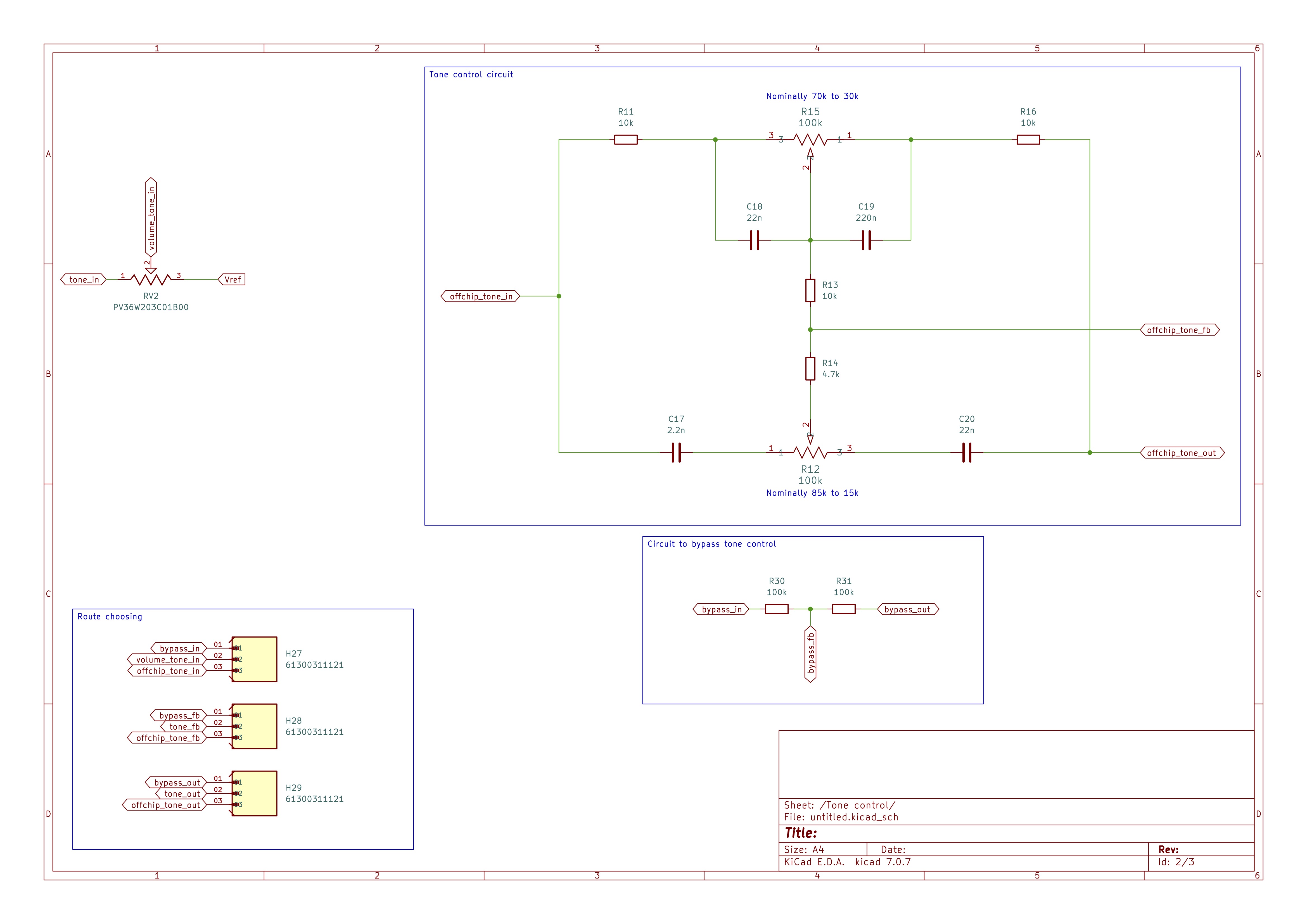
The tone control circuits are shown in Figure 1. c. By tuning the potentiometer in the RC filter, we can fine-tune the bass and treble parts of the music. Also, to achieve a completely flat frequency response, we can always bypass the tone control circuits. Besides, The volume can also be easily adjusted using a potentiometer.
The completed PCB board is shown in Figure 2