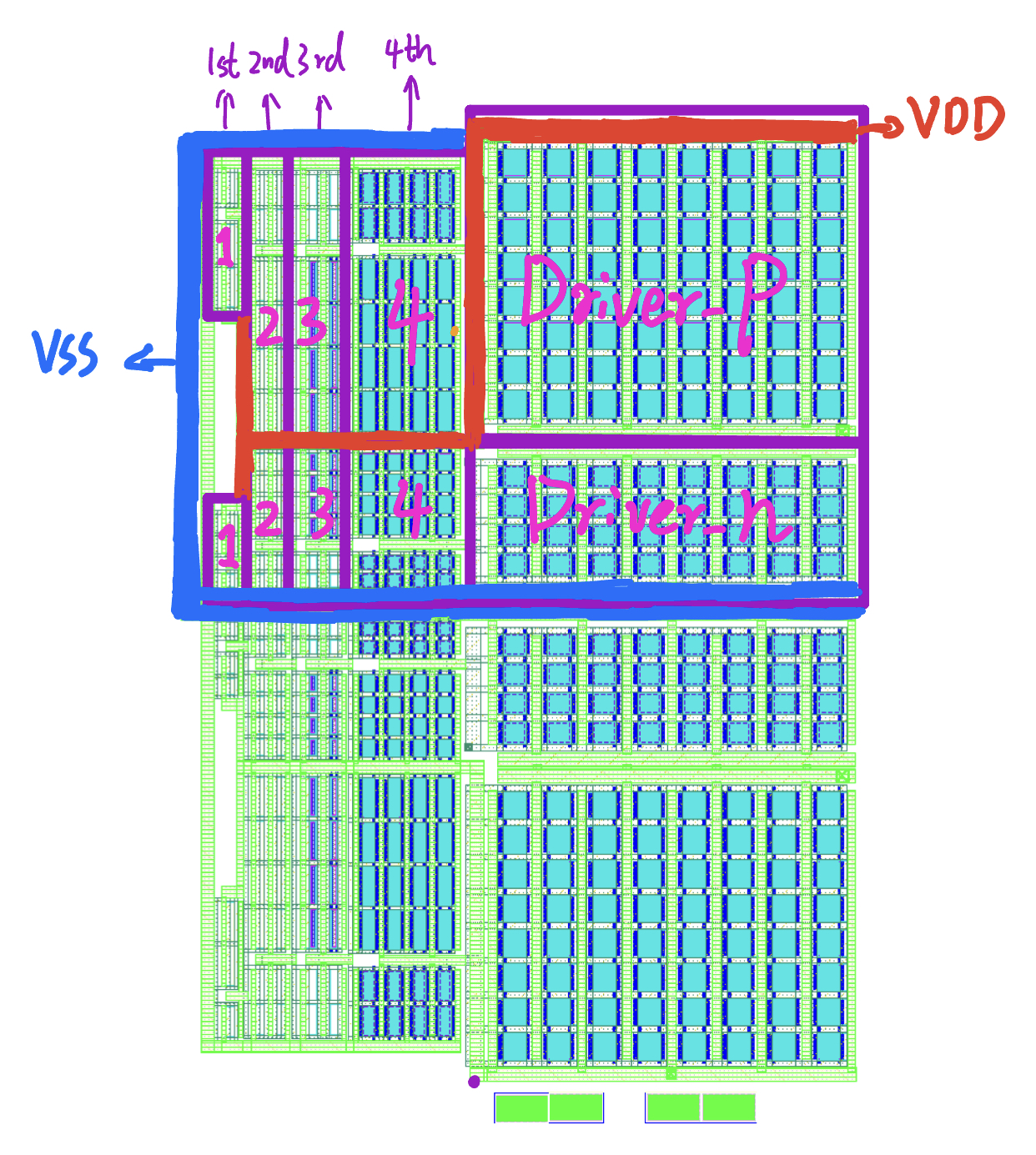
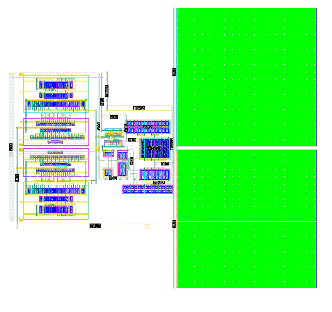
Layout

The overall layout of the chip is shown above. The floorplan of the whole signal chain is symmetric, with the output driver taking the most space to provide large driving strength. All the empty spaces left are filled with Decoupling caps to reduce ringing on the rails.
OTA
Single-ended to differential converter
Comparator
Triangle wave generator
Nonoverlapping generator
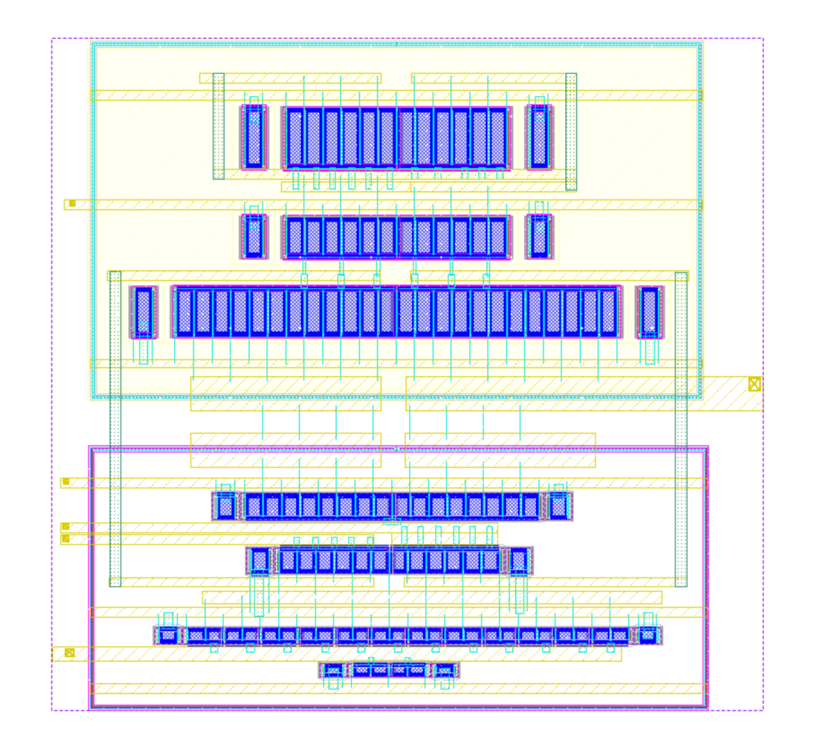
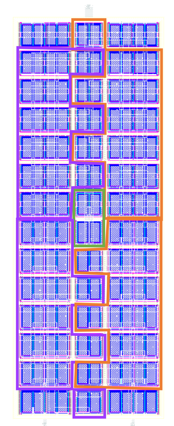
Current Mirror
To reduce mismatches, the current mirrors are laid out as close as possible. Additionally, the MOSFETs receiving the Iref are always in the center, while other MOSFETs are laid out symmetrically.
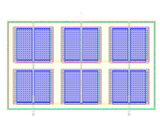
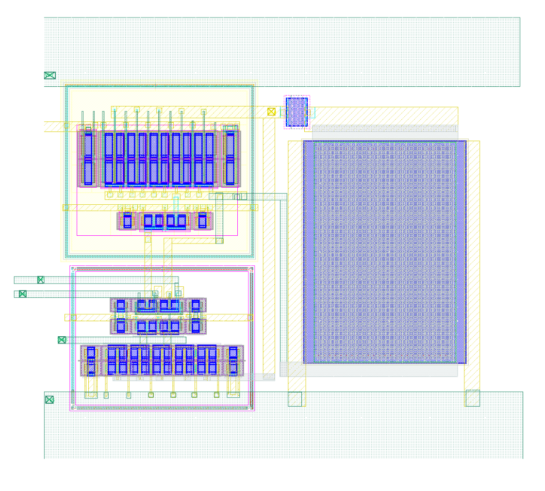
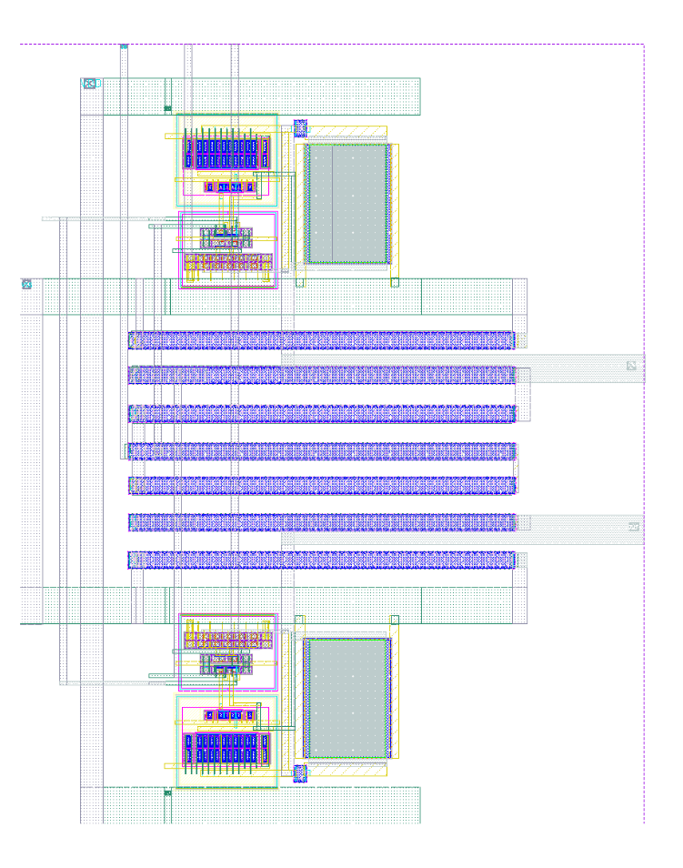
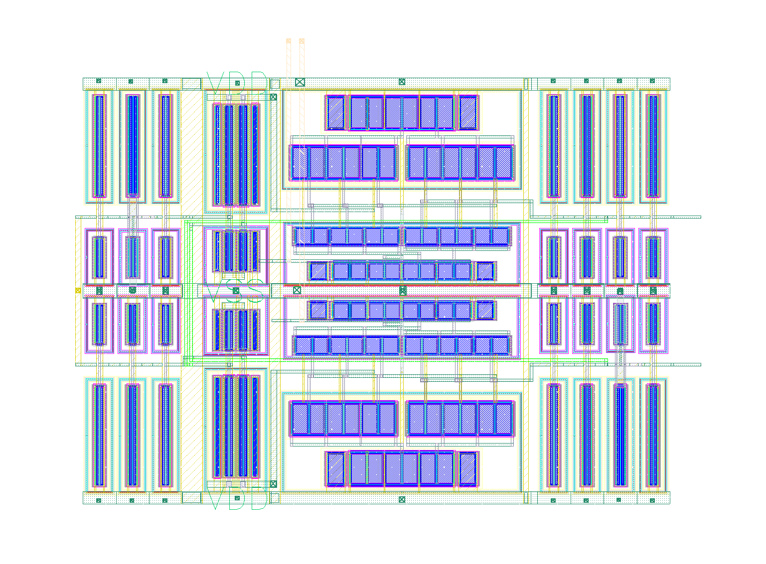
Output driver & pre-drivers