Circuits Design
OTA
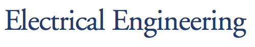
Figure 1 shows our two-stage OTA with miller compensation. This OTA is used in the integrator, single-ended to differential converter, and tone control network. It has an open loop gain of 74dB and 30MHz GBW.
Single-ended to differential converter
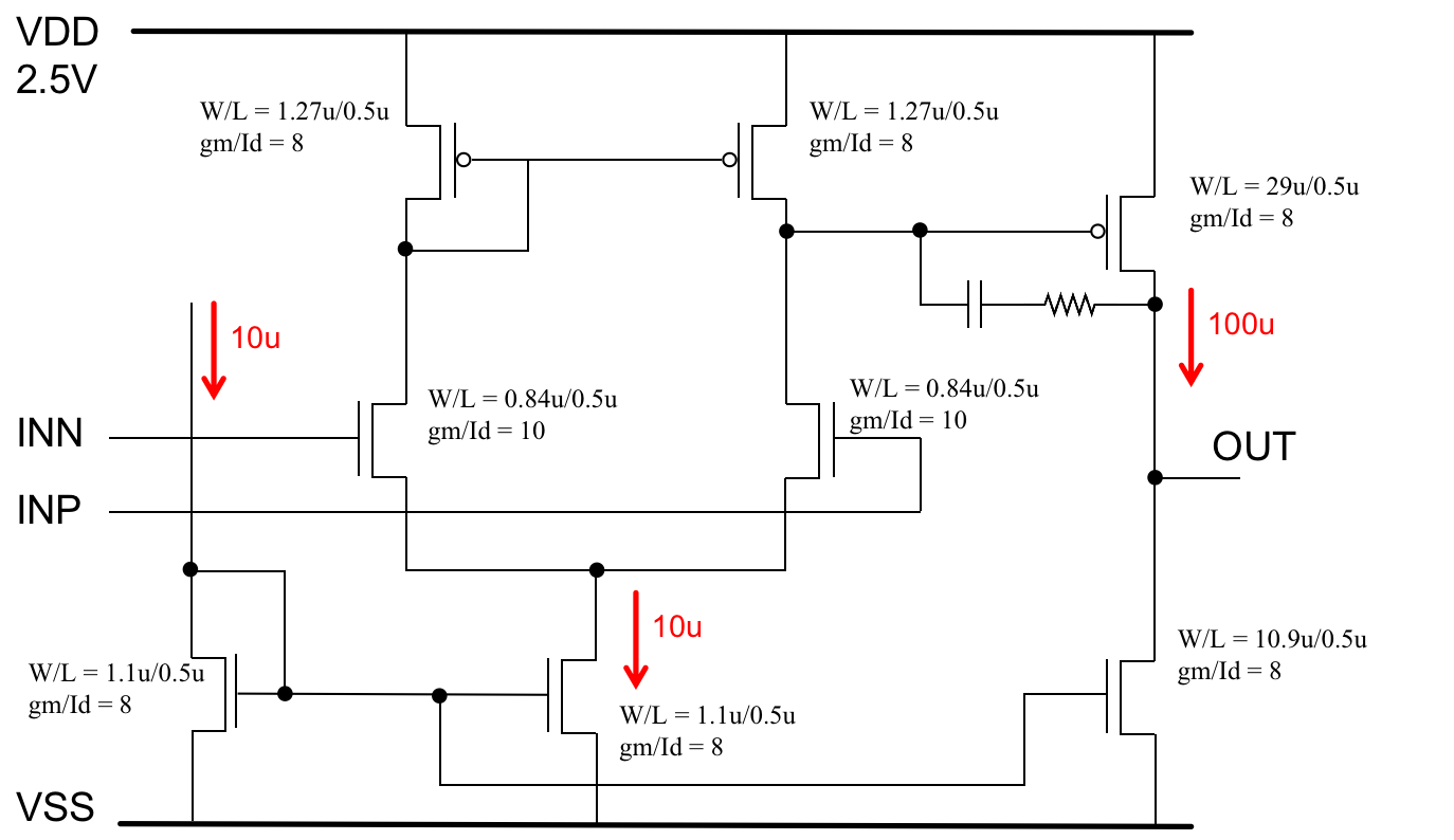
Figure 2 shows the single-ended to differential converter, the first inverting amplifier has a gain of 2, and it splits into two paths and generates two out-of-phase output signals.
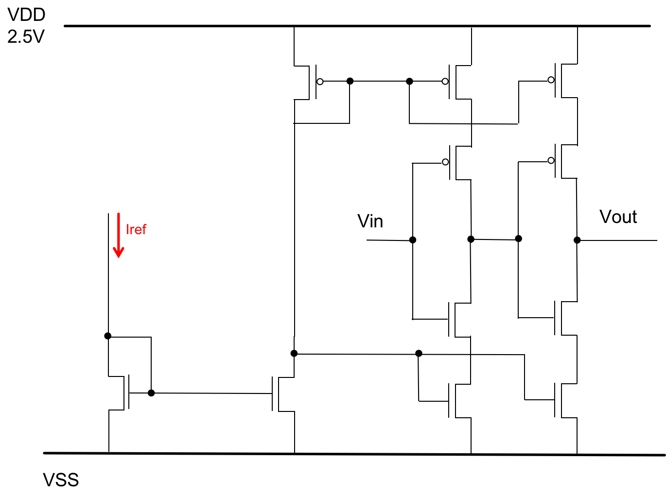
Comparator
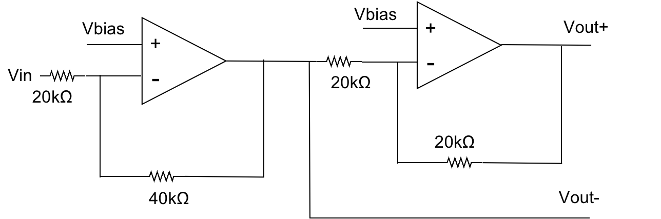
Figure 3 shows our comparator which is used in triangle wave generator and further pulse width modulation.

Triangle wave generator
The triangle wave generator first generates an uncontrolled triangle waveform with a relaxation oscillator, then compares it with two reference voltages with comparators. The comparator output is used to control a flip-flop circuit (SR latch) that holds the state of the comparator output to produce a square waveform. This square waveform is used as the input of the switches to generate a 500kHz triangle waveform.
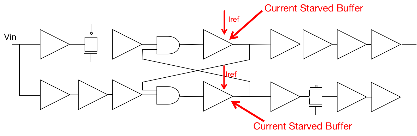
Nonoverlapping generator
To prevent nmos and pmos of the driver from working at the same time, we need to insert a dead-time generated by a non-overlapping clock generator before the signals that drive the high and low side MOSFETs. The delay can be implemented with a series of inverters and an additional current-starved buffer to adjust the dead time. We also added two transmission gates to make sure the delay in the two paths is exactly equal.
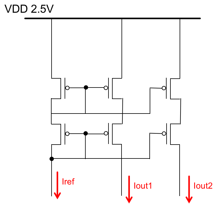
Current Mirror
Figure7 shows our cascode current mirror with off chip current reference. There are also current mirrors implemented using nmos to provide currents in opposite direction
Output driver
The driver could be treated as the most important part of the Class D audio amplifier, since it relates to the chip efficiency directly. When designing the driver, the first part is to determine the ratio between pmos and nmos. After running a simulation for a driver chain, a ratio of 2.6 would form the closest rising and falling time. In our design, the total size of nmos reaches 35360 um while the nmos is 13600 um in order to reach 95% efficiency. We rotate all pmos units and nmos units 90 degrees to decrease the usage of the high-parasitic impedance layer and also provide enough branches to hold some margins for the large driver current. The designed number of multipliers and fingers would make the layout symmetry under this special topology. At last, the parasitic resistance for pmos and nmos is 0.086 ohm and 0.071 ohm when driving an 8-ohm speaker.

Pre driver
As important as the driver, Pre-drivers are designed to drive the larger output driver. Figure 9 illustrates the pre-drivers for the output driver pmos. Their multiplier and fingers adopt same design strategy as the output driver. Also, the chain maintains almost Fan out of 4 to ensure a small delay. The total size of the pre-driver for the nmos is around 2.6 times smaller than those for the pmos to reach similar driving strength. The different nmos and pmos pre-drivers sizes cause a delay difference in picoseconds which can be ignored with respect to 20ns dead time.
