
Testing
The table below shows that the VCO-based design can support output voltage of upto 0.8V compared to 1.2V and provides lower dropout voltage of 100mV compared to 150mV for traditional design. It also has better load regulation: 8.8uV/mA compared to 29uV/mA while consuming lower quiescent power: 3.7uW compared to 30uW. The traditional design has lower settling time that is possible due to its higher bandwidth but it comes at a cost of higher power. Due to the critical nature of the zero for stability of VCO-based design, Cc and hence area is larger.
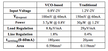
Figure below shows the transient response of the proposed LDO. This design has a slower settling time, but this can be further improved by increasing the loop bandwidth. A strategy would be to add extra circuitry to improve transient response by detecting the output spike. Another strategy would be to increase the charge pump current as well as to decrease Rz to increase the bandwith while keeping sufficient phase margin.