
Loop Analysis
The integrator used as an error amplifier creates a pole at DC in the loop transfer function and this results in a 20-dB roll-off at low frequencies (Concept and Architecture). This LDO is designed to be capacitor-free, so it is necessary to ensure that the dominant pole is placed at an appropriate location inside the loop to ensure stability. The Miller capacitor Cc is used to set the dominant pole at the gate of the power transistor. As it is inserted in the loop following the charge pump, it creates another pole at DC leading to 40-dB roll-off at low frequencies. Fig. 1 presents the linear model of the proposed LDO.
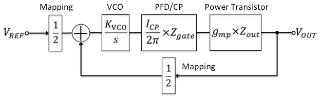
The open-loop transfer function is:
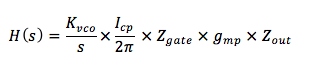
where Kvco is the gain of the VCO, Icp is the charge-pump current, gmp.× Zout is the gain of the power transistor and Zgate is the impedance at the gate of the power transistor, which is shown below:
In order to stabilize a loop with 2 poles at DC, it is necessary to bring a left-half plane zero before the unity gain bandwidth (UGBW) point to create a phase lead. Resistor Rz is placed in series with the Miller capacitor to create the zero at 1/(Rz.Cc). The parasitic capacitances of the power transistor, Cgs and Cgd, create the third pole. Due to the possible instability arising due to this pole, it is critical to place the zero in a way that maximizes phase margin of the loop. Fig. 2 shows the use of zero in this design to compensate the loop. The LDO is stable across all loads with the best case phase margin of 65 degrees at UGBW. The digital compensation using the 4-bit current DAC in charge pump allows external tuning of UGBW.
