PCB Design
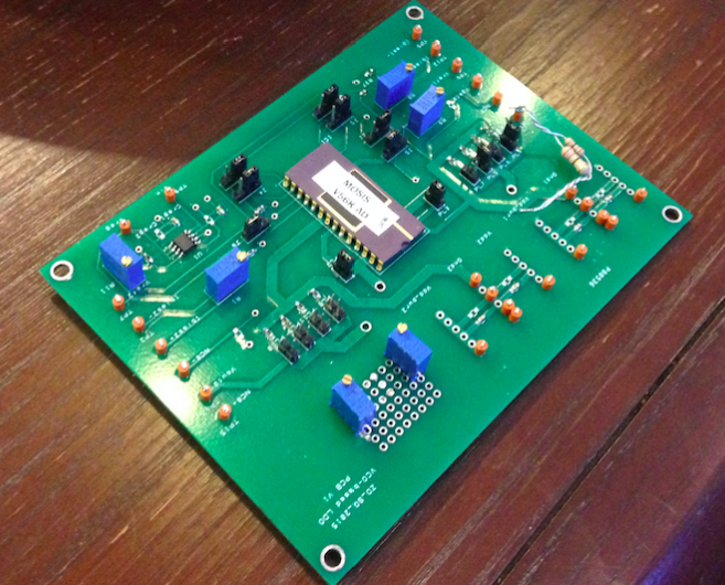
PCB was designed using a 2-layer board and fabricated with Advanced Circuits. We left plenty of space for probes and test-points as well as for potentiometers to set the bias current. Potentiometers were also used as load resistors for the regulators, and we tuned the resistance to get the desired load current. This helped us test for load regulation of the regulators.
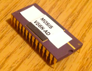
Below is the chip packaged in DIP-28 package.
Below is the PCB used for testing.