
Simulation Results
INA simulation
Single-ended OTA simulation
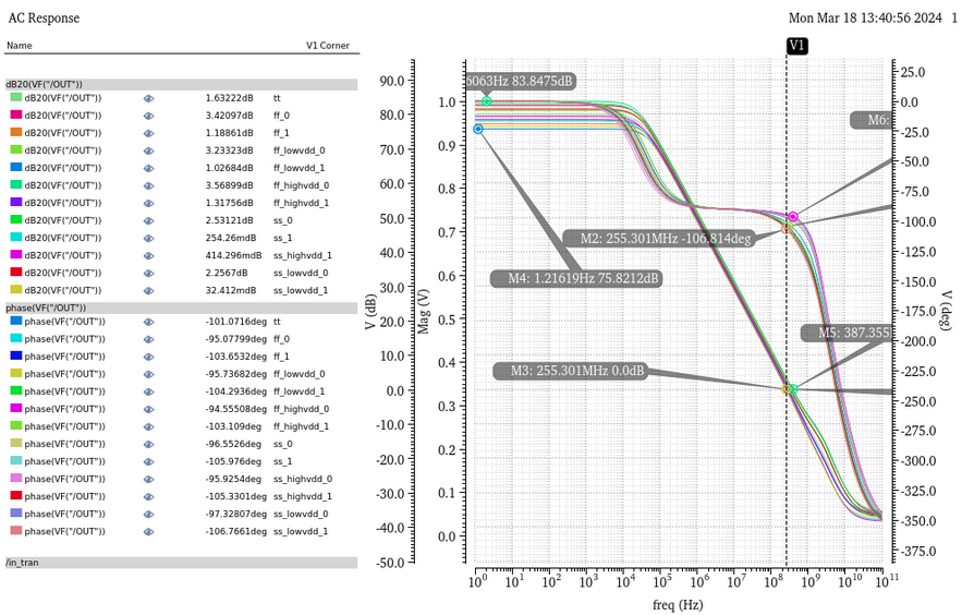
Fig 1. Single-ended OTA Simulation Results
The PVT sims above show quite a stable and robust response for the single-ended OTA design with a phase margin of about 74 degrees and a unity gain frequency ranging from 255MHz-387MHz. While for the worst DC gain is around 75dB which means it still can provide us with a less than 0.1% closed loop error.
INA gain simulation
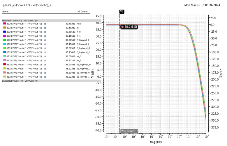
Fig 2. INA gain Simulation Results
Our design specification for the whole INA gain would be 90 (39.08dB) in total ideally. With the gain of 9 in the first stage and a cascade gain of 10 in the second stage. The results show that our INA gain under different corner simulations will have the worst low-frequency gain for 38.6 dB.
Fully-differential OTA simulation
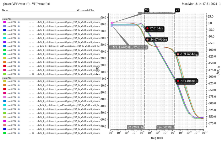
Fig 3. Fully-differential OTA Simulation Results
Our design specification would be 80dB gain for fully-differential OTA while in reality under different PVT conditions, the worst DC gain response would be only 77 dB. However, this can still give us a closed-loop gain error under 0.1%. The phase margin we can see above is quite close to 71dB, which is stable enough for our system. The GBW would be around 200MHz, however, we don't care about that much on GBW since ECG really works on a low-frequency design.
Mismatch simulation for INA
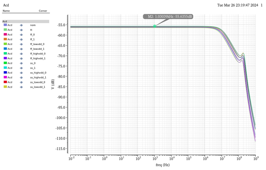
Fig 4. 0.1% R Mismatch Simulation Results
What we can see from here is 0.1% error on the ratio of feedback resistor on the second stage will give us a CMRR of about 55+38 =93dB.
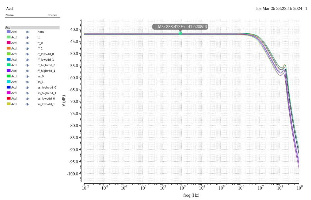
Fig 5. 1% R Mismatch Simulation Results
Similarly, with 1% mismatch shown on the feedback resistor of INA will give us a CMRR of about 41+38=79dB.
PGA simulation
PGA has 4 different gains. We apply sine wave input, and the output is shown below.
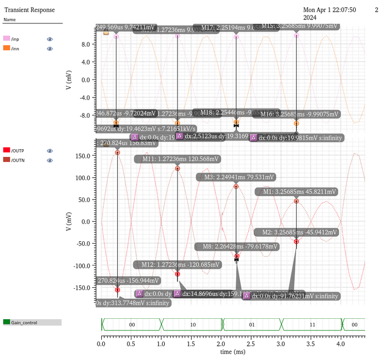
Fig 6. PGA Transient Simulation Results
We also run AC simulations for the PGA. The gain is 13.24dB, 18.32dB, 21.71dB, and 23.99 dB.
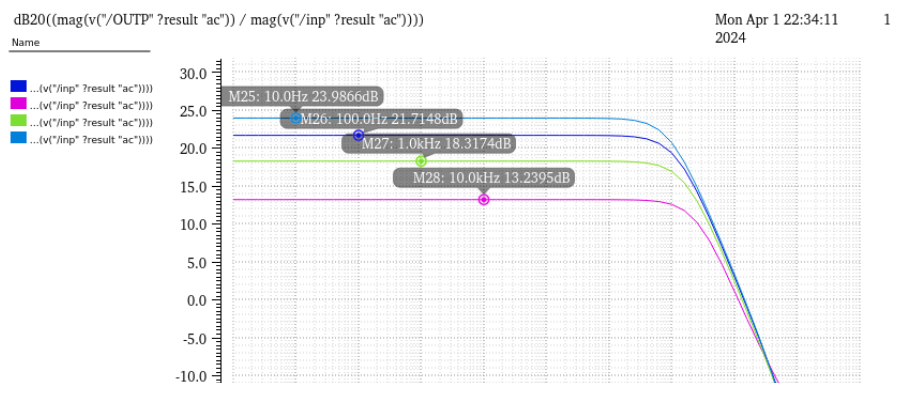
Fig 7. PGA AC Simulation Results
Freq Divider Simulation
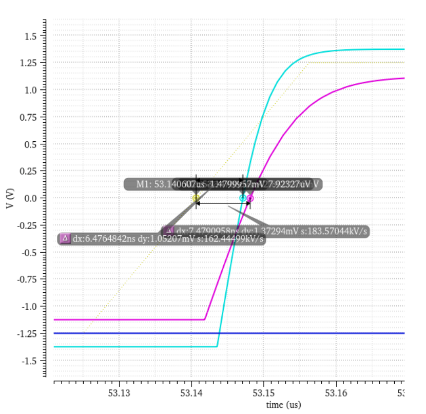
Fig 8. Freq Divider Simulation Results
As shown in the Figure, the delay of the frequency divider doesn't change too much under different PVT conditions. The delay varies from 6.5 to 7.5ns.
ADC Simulation
SAR Simulation
SAR logic block shifts logic high from the MSB to the LSB, which is shown in the transient simulation result below. We also want to make sure that the transition time of the SAR is short because a longer transition time is not acceptable. The transition time varies from 3.63ns to 6.39ns under different PVT conditions.
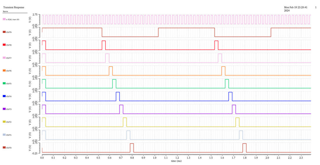
Fig 9. SAR Simulation Results
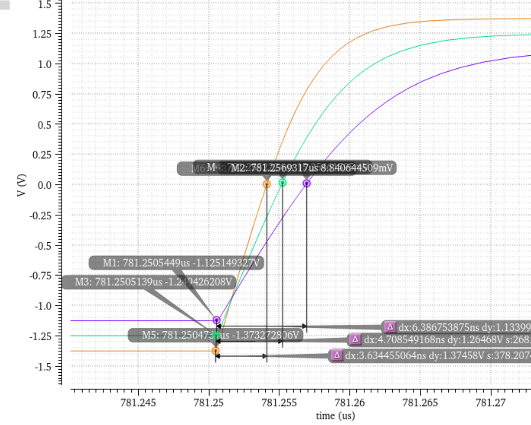
Fig 10. SAR Transition time Simulation Results
StrongArm Comparator simulation
To simulate the comparator, we apply a very slow ramp input and measure the offset when the comparator's decision changes. We ran 100 samples of the Monte Carlo simulation and the result is shown below. The standard deviation is 1.875mV. 3 sigma is around 1 LSB, which is tolerable.
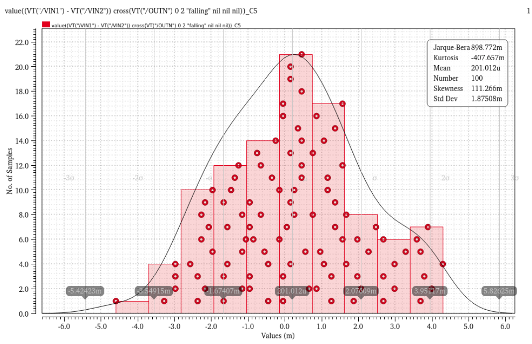
Fig 11. Monte Carlo Simulation Results
We also measure the decision time of the comparator under different PVT conditions. The decision time ranges from 485ps to 846ps, which is enough for a 10KHz sampling rate ADC.
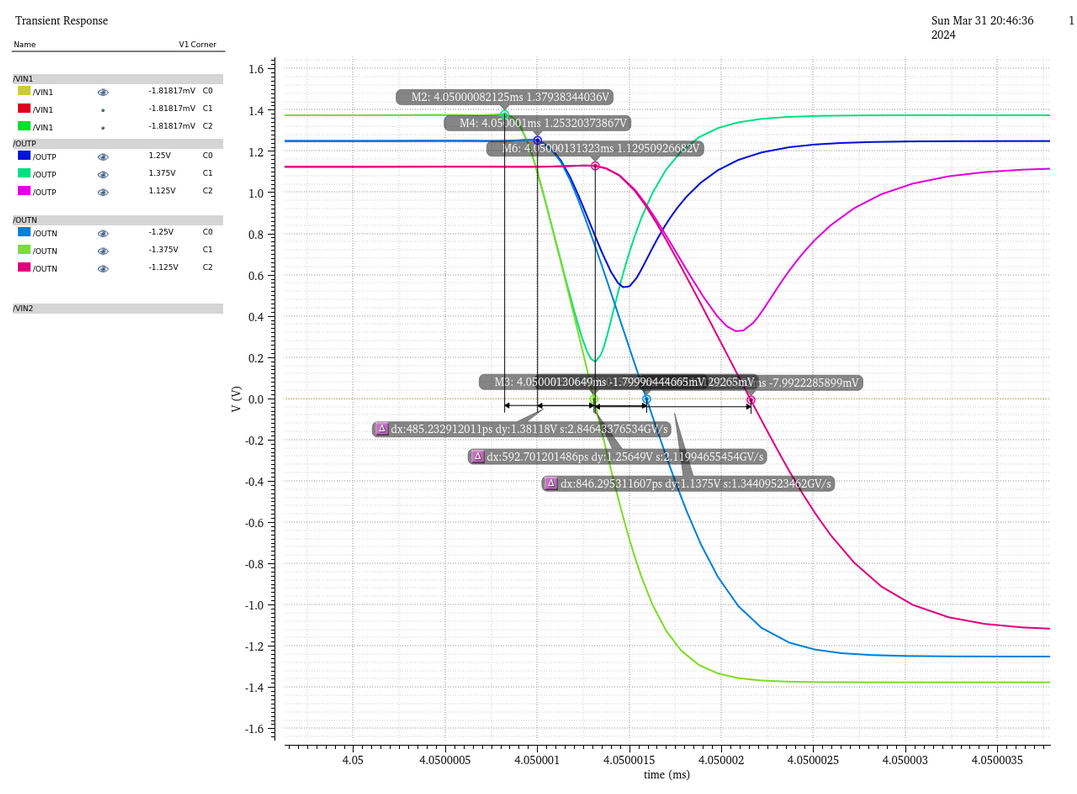
Fig 12. Decision Time Simulation Results
Sample & Hold simulation
The transient simulation of the sample and hold circuit is shown below. The hold pedestal is about -0.5mV, voltage droop is about -1mV. Most of the offset in single-end design can be counteracted because our structure is differential.
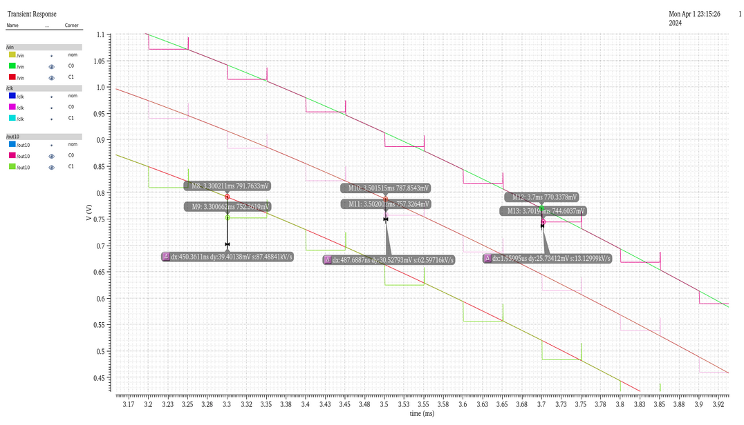
Fig 13. Sample & Hold Simulation Results
Overall ADC simulation
We connected an ideal DAC to our ADC in the test bench. The figures below show our ADC DFT simulation setup and results. The input signal's frequency is finely selected to avoid deterministic quantization noise and discontinuities. Under SS_rtmom/SF_25/80C, the ENOB is 9.958bits. Under TT_rtmom/TT_25/27C, the ENOB is 9.982bits.
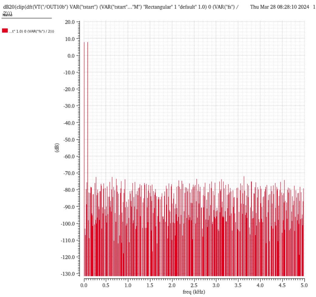
Fig 14.DFT Simulation Results
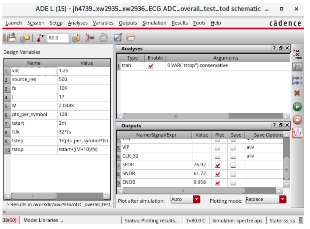
Fig 15.DFT Simulation Setup
The transient result of a slow input ramp shows that there is no missing code.
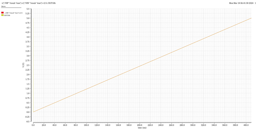
Fig 16.Ramp Simulation