
IC Design
INA
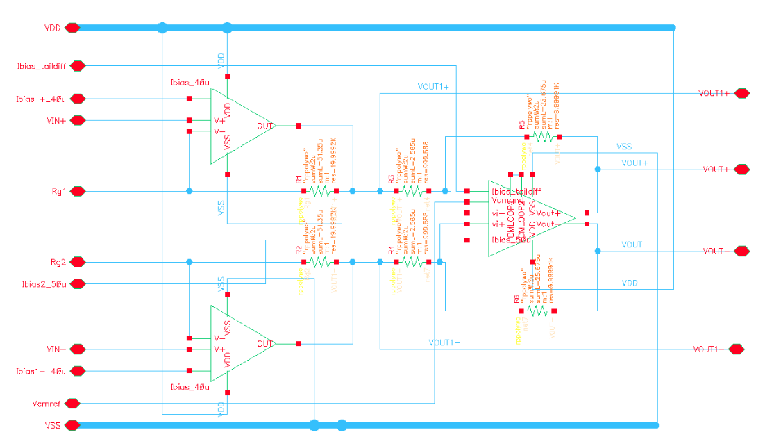
Fig 1. INA Schematic
The whole schematic of the Instrumentation Amplifier is shown above. Overall, it is a symmetrical structure. The first stage consists of two OTAs with a PMOS input on the upper and lower sides, and the second stage is a fully differential two-stage OTA with NMOS input pair, common-mode feedback (CMFB) to stabilize the output DC value. For the two Single-ended OTA, we need a 40uA current bias. The PMOS input is selected to have better noise performance under the same size. While for the 2nd stage OTA, we are using the fully differential structure in order to get better output range and reduce noise. The whole INA would have a gain of 90 in total with 1st stage gain of 10V/V and second stage gain of 9V/V. Due to time constraints, we did not design a cascode structure for each OTA. In addition, the CMRR is another thing that we care a lot about. When amplifying biological signals such as ECG signals, the amplitude itself is very small, while 60Hz noise is everywhere in the laboratory and in life. For a fully differential instrumentation amplifier, in theory, as long as the common-mode rejection ratio is high enough, the stronger the suppression of common-mode noise, the ECG signal will be correctly amplified after passing through the instrumentation amplifier, and the unwanted common-mode noise will be filtered out. From Biological journals and papers, a good INA should reach CMRR more than 90dB and that would be our target in this design.
Fully-Differential 2-Stage OTA
For fully-differential 2-stage OTA with CMFB above, we do use two bias currents here. One for the OTA and one for the error amplifier, which are both 50uA. While for the CMFB of the amplifier, we do need a relatively large feedback resistor pair in order to not lower much DC gain of the two stage OTA, the OTA is designed to be with a DC gain of 10000 V/V(80dB). While for the error amplifier, it is a 5 transistor amplifier, with low gain and wide bandwidth, since its function is to provide feedback to fix the output voltage to reference voltage (1.25V), we don't want to spend much power (more current and more gm) on this error amplifier. The total current consumption would be approximately 350uA with 50uA coming from the error amplifier.
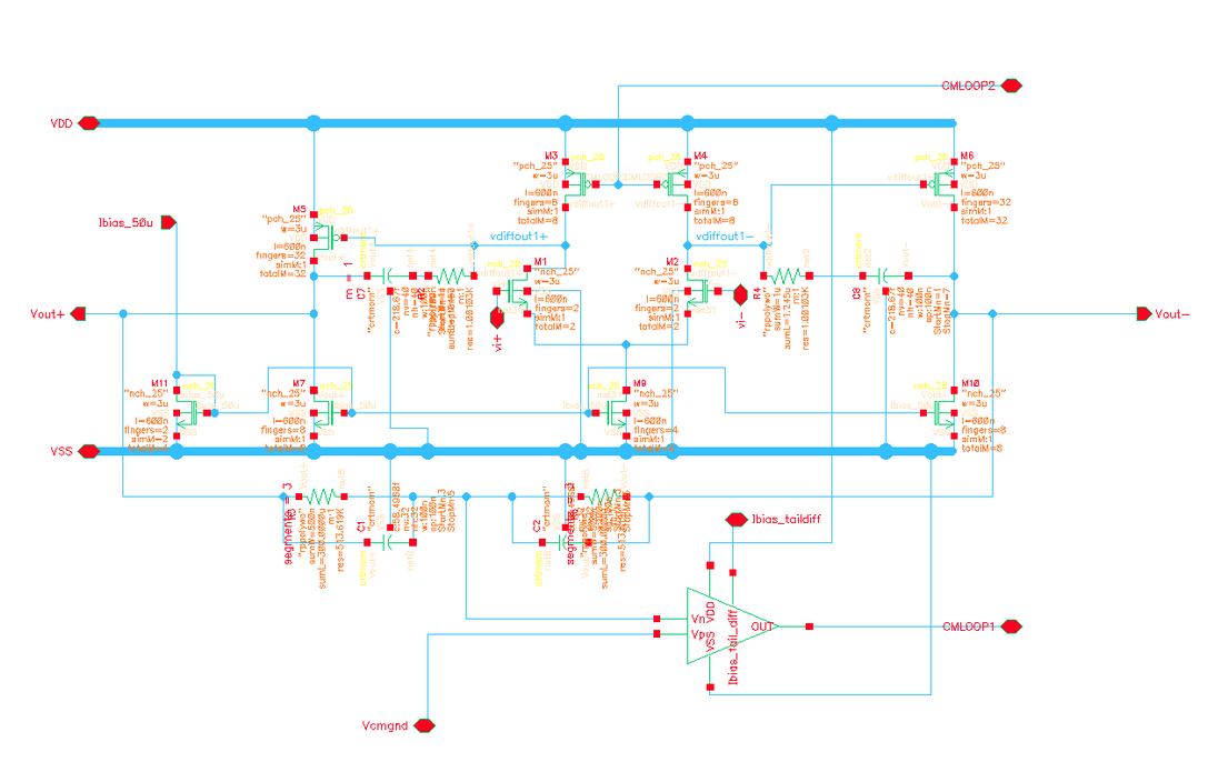
Fig 2. Fully-Differential 2-Stage OTA Schematic
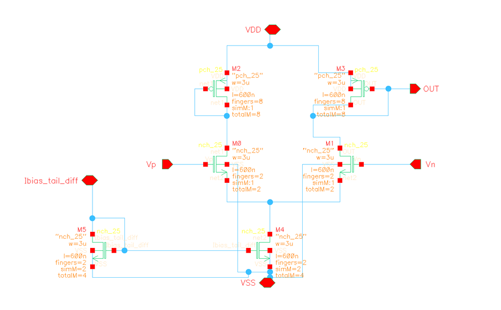
Fig 3. Error Amplifier Schematic
Single-ended 2-stage OTA
For this Single-ended two stage OTA, PMOS input pair is chosen for better noise performance under same sizing. We hope to achieve enough DC gain (80dB) to ensure that our feedback circuit error is within 0.01%. At the same time, we hope to minimize our bandwidth (GBW) to minimize high-frequency noise. Therefore, our sizing is to use a relatively small transistor. The current ratio of stage 1 and 2 would be approximately 1 to 2 and the total current consumption of this stage would be 280uA.
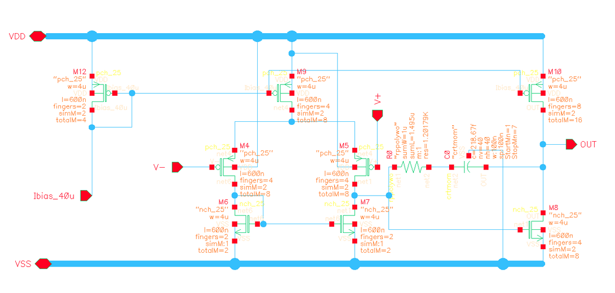
Fig 4. Single-ended 2-stage OTA Schematic
PGA
PGA reuses the differential OTA in INA as mentioned above. To modify the gain (4x, 8x, 12x, 16x), 2 digital control bits are implemented by complementary MOS switches, which can short part of resistors. Multiple gains can fit different ECG input strengths.
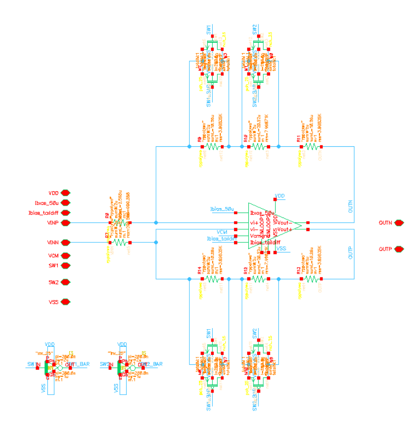
Fig 5. PGA Schematic
10-bit SAR ADC
SAR ADC implements binary search, which divides the voltage range into two regions and checks which of the two regions the input voltage belongs to.
The whole schematic of 10-bit differential SAR ADC is shown in Fig. 6, which contains sample & hold, comparator, CDAC, frequency divider, and SAR. The ADC operates at 10 kS/s sampling rate, with 320 kHz work frequency. It uses 2.5V positive reference voltage, 0V negative reference and 1.25V common mode voltage, corresponding to 2.5V power supply. With the fully differential structure, the full scale is 5V, which means LSB = 5V/1024 = 4.88mV. To improve clock driving ability and reduce glitches, CLK buffers (inverters) are added.
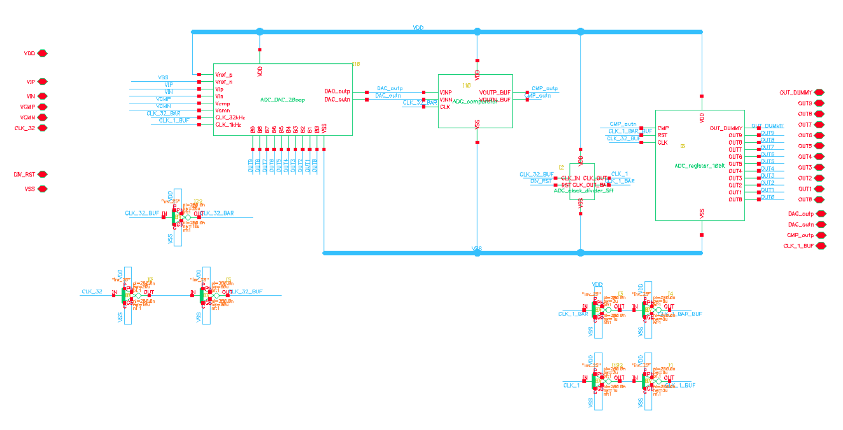
Fig 6. ADC Schematic
Frequency Divider
The ADC works on 320 kHz, which is provided by an external generator. ECG signal is sampled by 10 kHz, which is generated from 320 kHz clock by a frequency divider consisting of 5 cascade flip-flops.
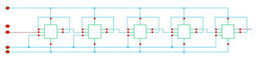
Fig 7. Clock Divider Schematic
Sample & Hold
Because ECG signal is mainly in 1~150 Hz, a simple 2nd-order bandpass filter can avoid aliasing of the ADC with 10 kS/s sampling rate. The bootstrapped sampler implements a charge pump, which allows sampling switch's gate to swing to 2*VDD and ensures that Ron and charge injection have less dependence on Vin's value. Moreover, each bit's switch has corresponding size as capacitors to get the same settling time and ratio of charge injection, which reduces glitches and nonlinearity. At logic high of 10 kHz, the circuit samples input signal; at low, hold the voltage in capacitors of CDAC for comparison.
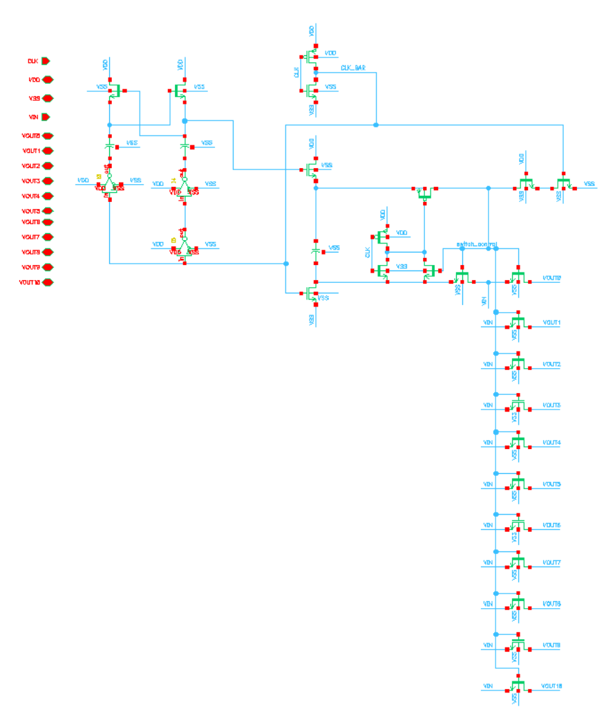
Fig 8. Sample & Hold Schematic
Successive Approximation Register (SAR)
SAR has 10 bits register to store comparison results and 1 dummy bit to be the valid flag. Each bit consists of a flip-flop with reset and a MUX. At the hold phase, there are 16 cycles for comparison (10 get results, 6 lock data for reading). When the dummy bit goes high, the microcontroller can read 10 digital bits for display. Additionally, the non-redundant structure has multiple OR gates to lock previous bits instead of adding 1 row of register to store, which saves area and power.
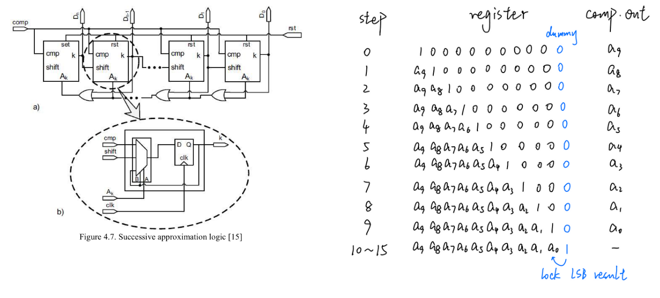
Fig 9. SAR Logic
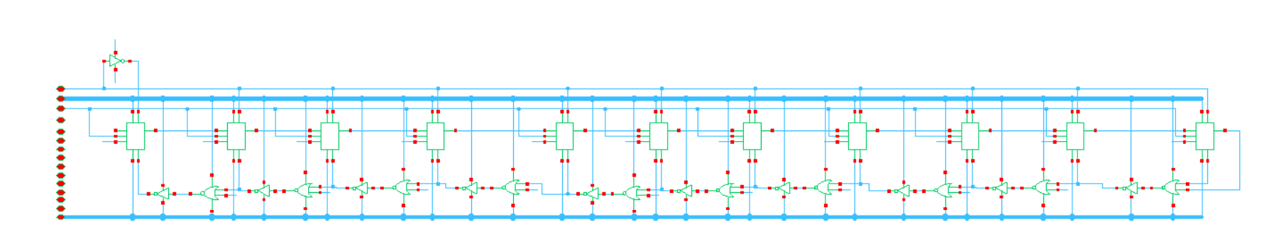
Fig 10. SAR Schematic
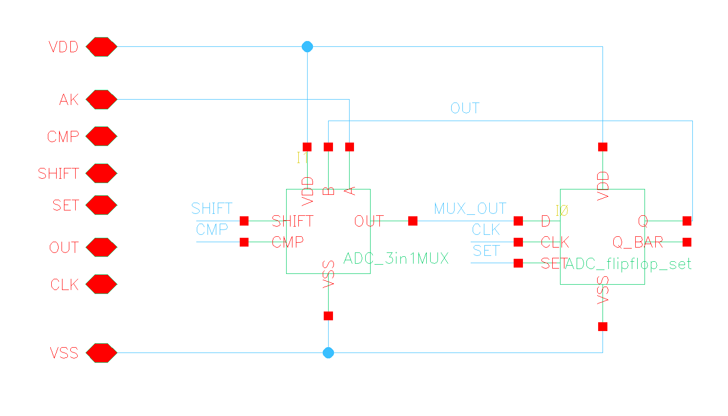
Fig 11. SAR Unit Schematic
Comparator
The StrongArm Latch structure is applied to the dynamic comparator. Buffers (not in figure) are added to output to ensure complete logic high and low, and also avoid effects from other blocks. StrongArm provides lower offsets and has lower power consumption. The precharge nodes (source of M6, M9) avoid hysteresis. To reduce offset, the input pair (M7, M10) should have a larger size, but trade-off with larger parasitic, which affects CDAC's charge distribution and linearity.
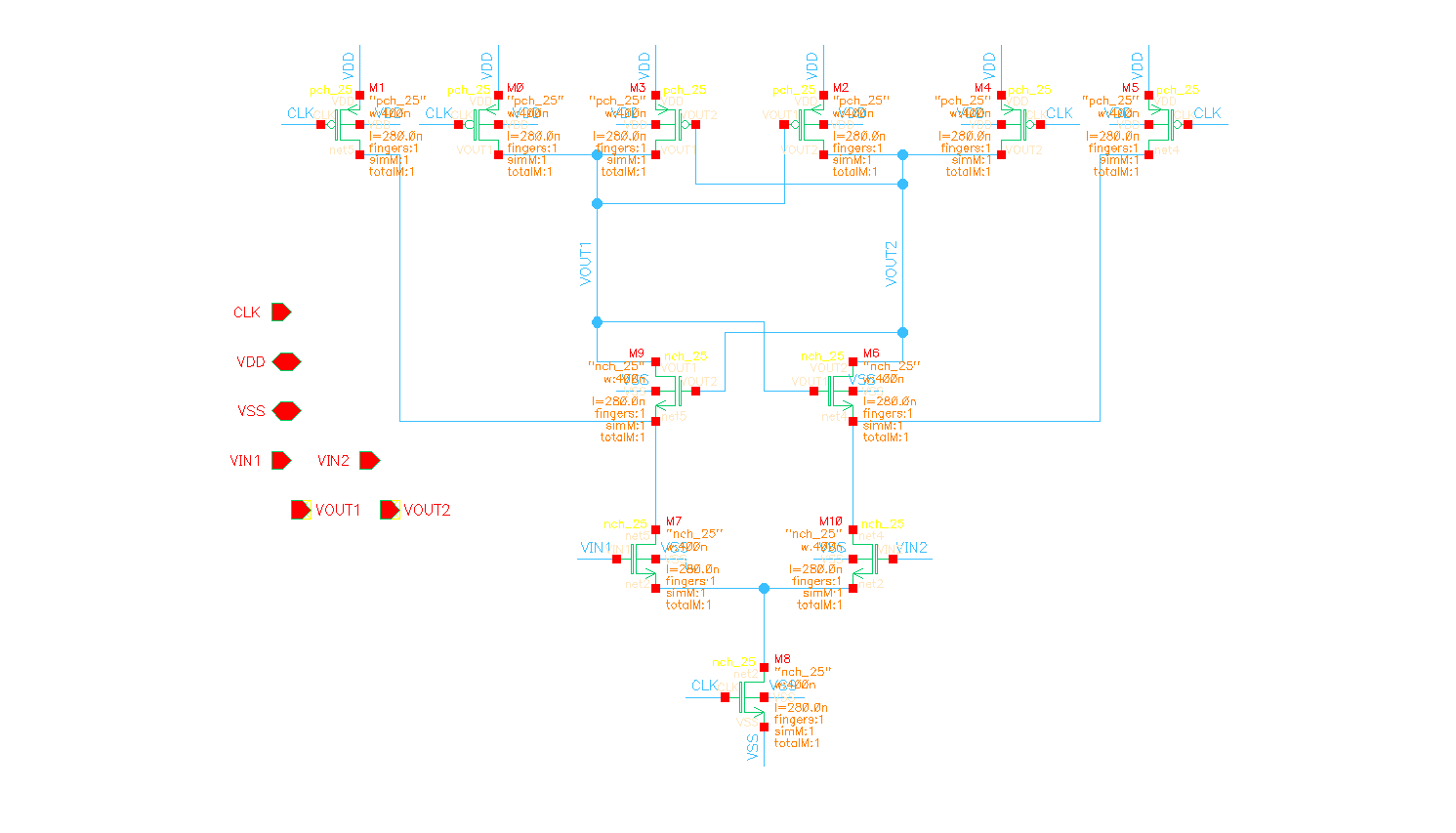
Fig 12. Comparator Schematic
Capacitive DAC
A 10-bit differential CDAC consists of an array of individually switched binary-weighted capacitors and stores input voltage. The amount of charge upon each capacitor in the array is used to perform the binary search in conjunction with the comparator and SAR.
Bottom-plate sampling needs common mode voltage (1.25V) and converge differential input to this level, which is more stable and fits non-rail-to-rail comparator's input. Compared to top-plate sampling, the disadvantage is that an extra MSB is added and the capacitance is twice that of upper-plate. Moreover, it is recommended to build binary-weighted array by switch-capacitor units, to keep the same size and settling time for each bit. The unit capacitor value is determined by kT/C < (0.5*LSB^2)/12, which means kT/C noise should be smaller than half of quantization noise.
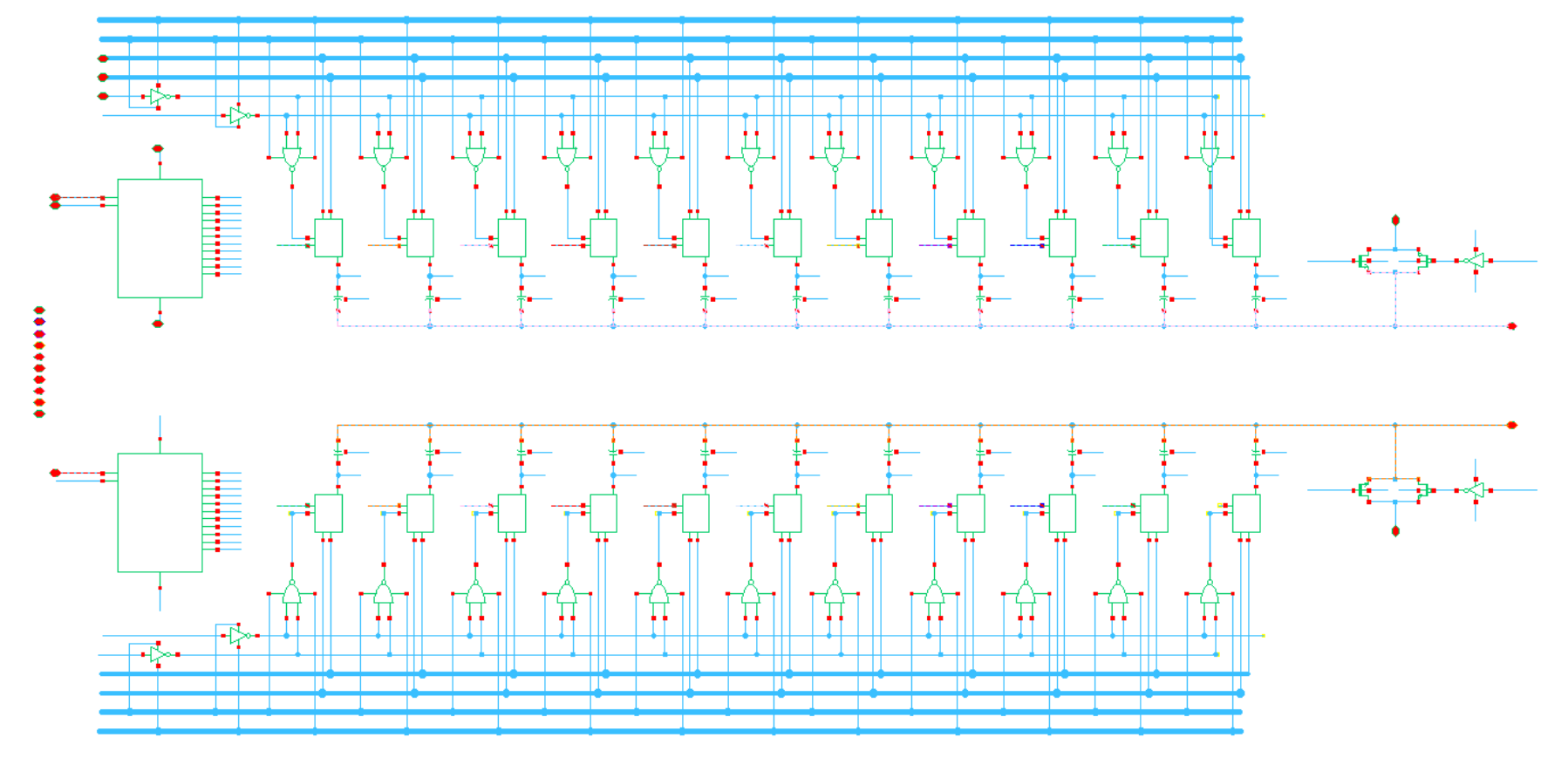
Fig 13. CDAC Schematic
Reference voltage uses an independent power domain instead of VDD and VSS to reduce noise. Switches are controlled by comparator's results and connect positive or negative references to each bit.
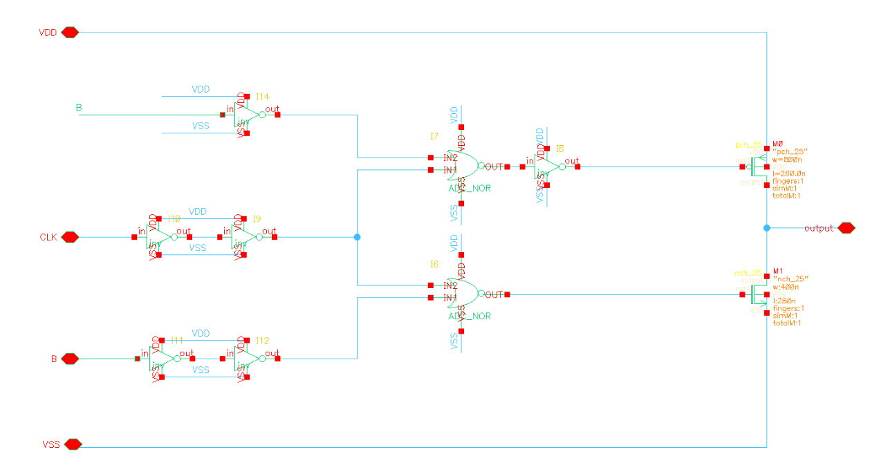
Fig 14. Reference Switch Schematic