
IC Layout
INA
In general, we hope that the layout of the entire INA remains highly symmetrical (from various angles), because this is a fully differential input and differential output INA, and we hope that the symmetry performance will minimize its offset. We made dummy devices for the input pair and the amplifier stage to keep these tubes in the same environment. At the same time, for the feedback resistor, the resistance value and ratio of the second stage need to be controlled very accurately. The mismatch of the second stage resistance will cause our CMRR to deteriorate rapidly, so we also need to ensure the consistency of the environment of the resistors and make dummy resistors. Two single ended OTAs are located on the two sides while the fully differential one is in the middle.Symmetry is the first priority of design. As for area saving, we did not consider it too much due to time constraints. The total current consumption is not that much so we can just use standard size metal for routing.
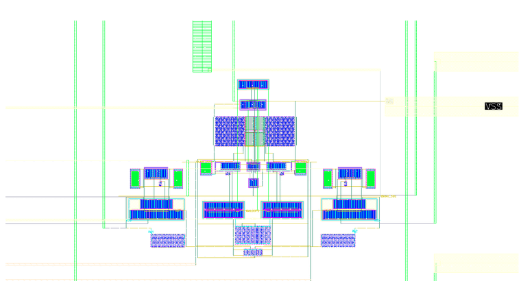
Fig 1. INA Layout
PGA
In general, for PGA, the core of layout is still symmetry because the next-stage ADC needs to accept fully differential input. We need to ensure that the offset of PGA is as small as possible. The second thing is about the resistance of PGA. Because the accurate amplification value is very important to us, we still use dummy resistors to ensure that their environments are consistent. Because the PGA uses the fully differential 2-stage OTA in the INA design, the layout will interact with other modules on this basis. Also due to time constraints, we have reserved sufficient space for us to correct and adjust the layout.
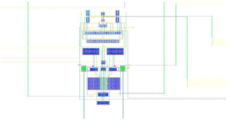
Fig 2. PGA Layout
10-bit SAR ADC
The whole layout of 10-bit differential SAR ADC is shown in Fig. 3. For better differential performance, the layout is symmetrical and follows signal flow’s direction. Wide wire of power supply can provide sufficient current. The power supply and CLK are far from analog input to avoid coupling noise.
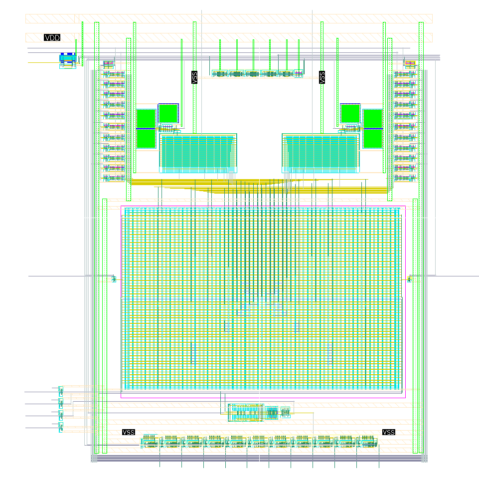
Fig 3. ADC Layout
Frequency Divider
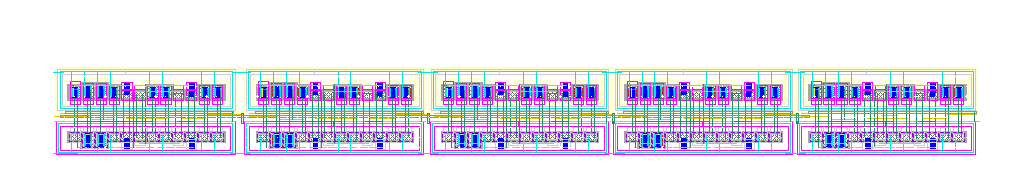
Fig 4. Clock Divider Layout
Sample & Hold
To connect one of Pmos body to source instead of VDD, a separate guard ring is created.
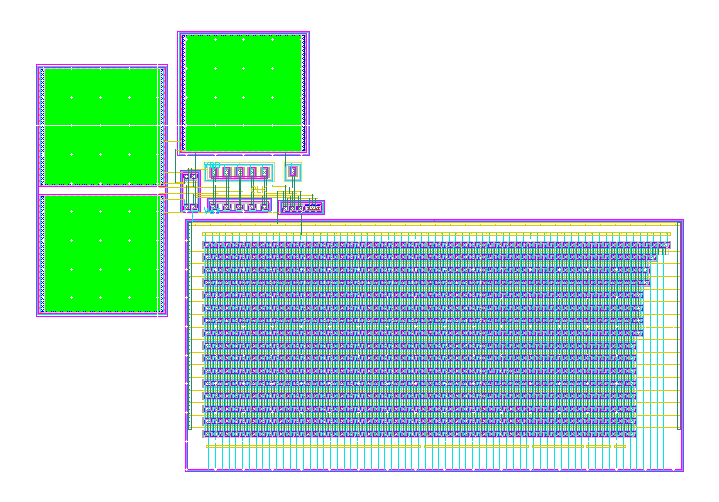
Fig 5. Sample & Hold Layout
Successive Approximation Register (SAR)
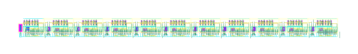
Fig 6. SAR Layout
Comparator
For smaller offset, transistors matching (especially input pair) is important. Interdigitated fingers and dummy devices are applied.
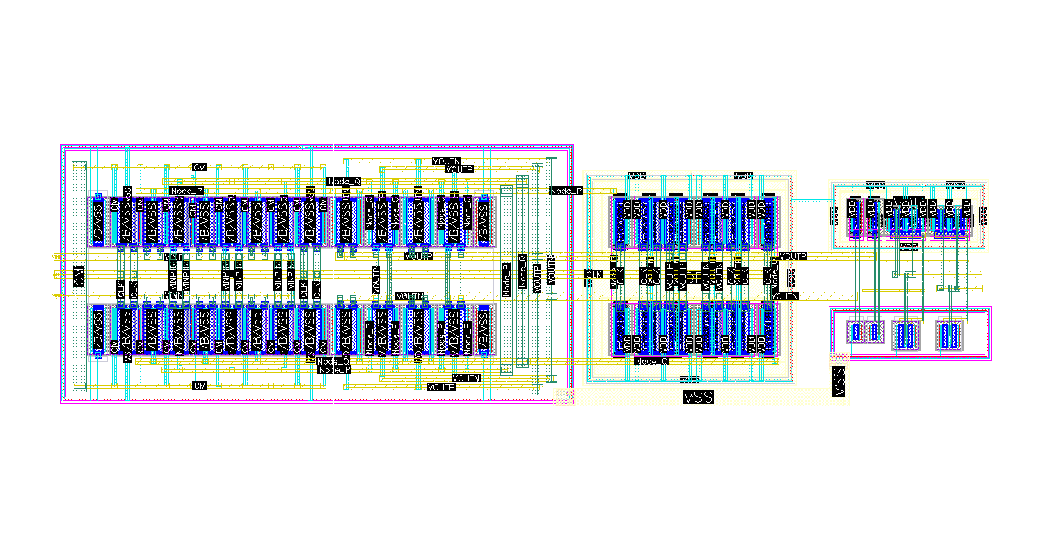
Fig 7. Comparator Layout
Capacitive DAC
The capacitor array is center symmetrical for better matching, and ensures the same parasitic in each unit capacitor.
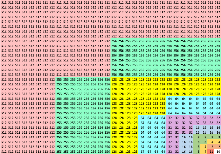
Fig 8. 1/4 of Capacitor Array Arrangement
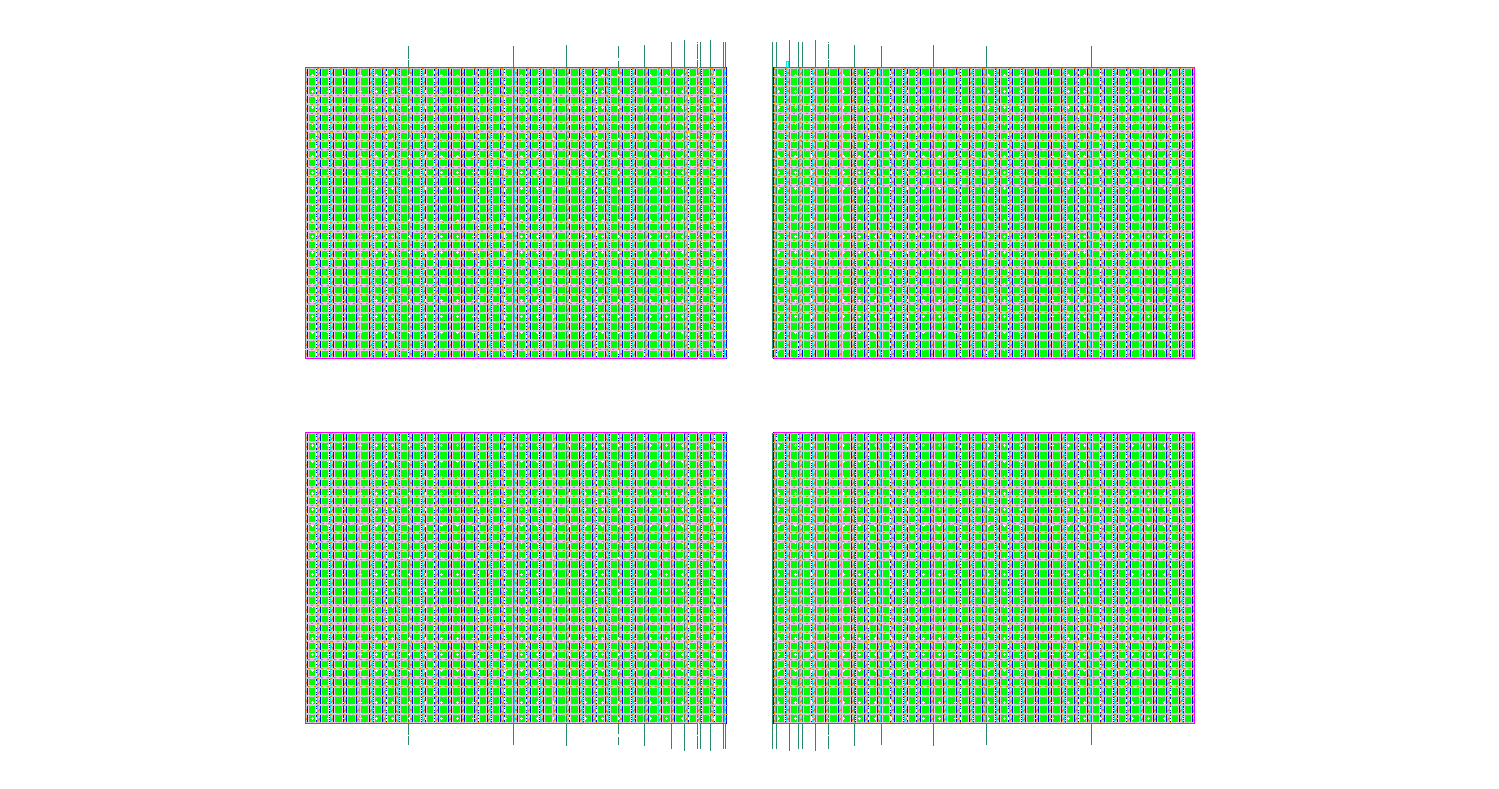
Fig 9. Capacitor Array Layout