
PCB design
In order to verify the functionality of the ECG measuring system, we designed a 2-layered PCB using Kicad. An overview of our PCB is given in Fig. 1 and Fig. 2.
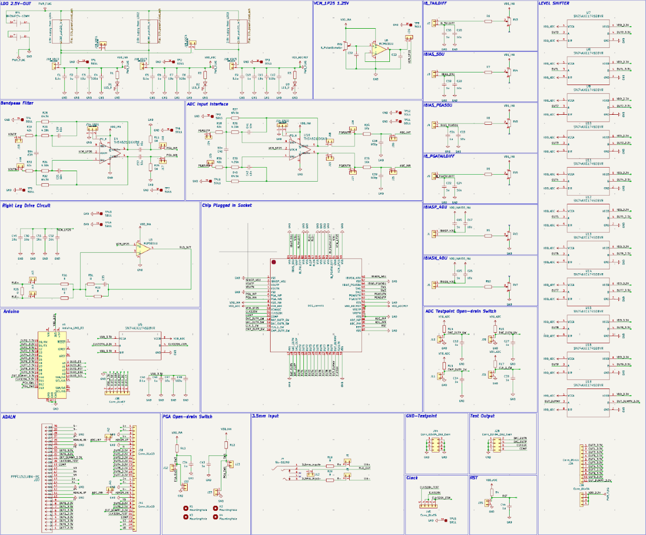
Fig 1. PCB Schematic
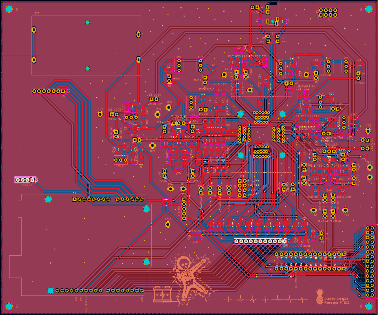
Fig 2. PCB Layout
POWER CIRCUITRY
There are several different power sources on the PCB. The first source is batteries, providing 3V to 3 LDOs on the PCB. Each LDO will generate 2.5V supply for the chip, as shown in Fig. 3. LDO's output voltage can be tuned by adjusting the resistor feedback of the LDO. The second source is 3.3V supply for the level shifter, which is provided by the Arduino.
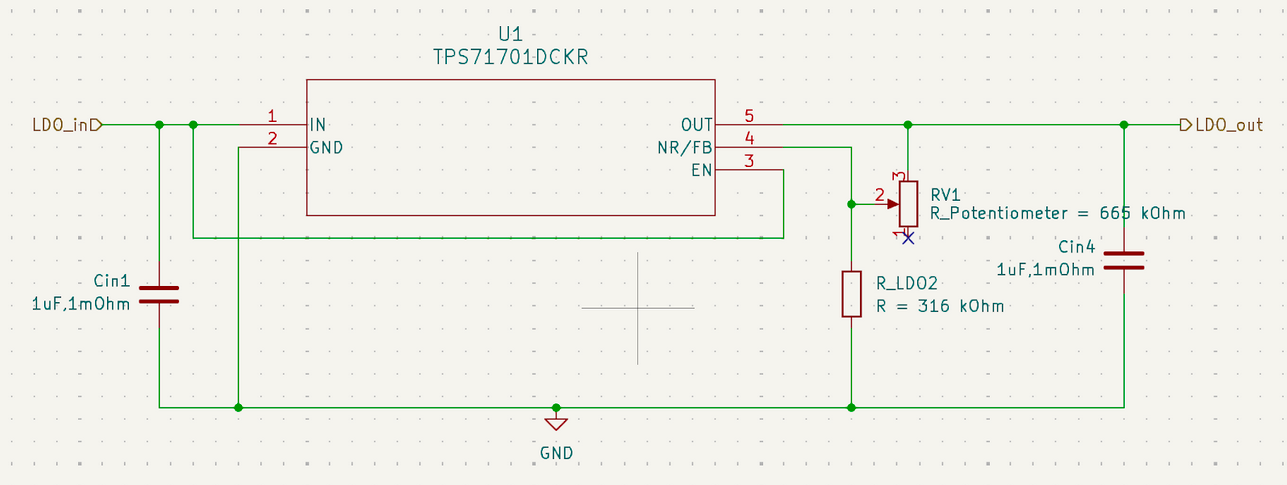
Fig 3. LDO Schematic
For each LDO, we add multiple decoupling capacitors with different values. Three red LEDs are also included as our power indicators, as shown in Fig. 4.
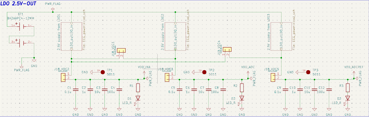
Fig 4. LDOs Schematic
Common mode voltage supply
We used an opamp as a unity gain buffer to generate our 1.25V common mode voltage. The output voltage can be tuned by adjusting the potentiometer, as shown in Fig. 5.
Fig 5. Common Mode Voltage Supply Schematic
BIAS CIRCUIT
Bias currents are provided by adjusting the potentiometer. Decoupling capacitors are also added to prevent sudden changes.
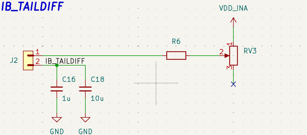
Fig 6. NMOS BIAS Schematic
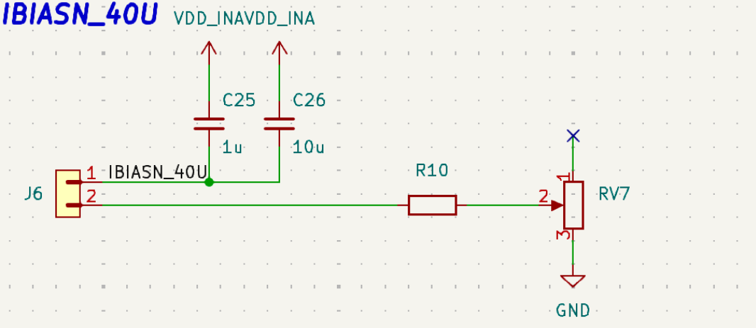
Fig 7. PMOS BIAS Schematic
LEVEL SHIFTER
Eleven bidirectional level shifters are used to transfer 2.5V output from the on-chip ADC to the 3.3V microcontroller input.
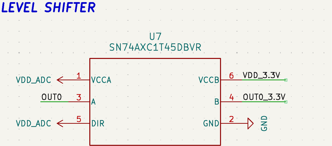
Fig 8. Level Shifter Schematic
BANDPASS FILTER
As shown in Fig. 9, we design an off-chip bandpass filter to filter out the DC offset and high-frequency noise of the INA output. Differential Rauch low pass filter topology and RC high pass filter topology are used to implement the bandpass filter.
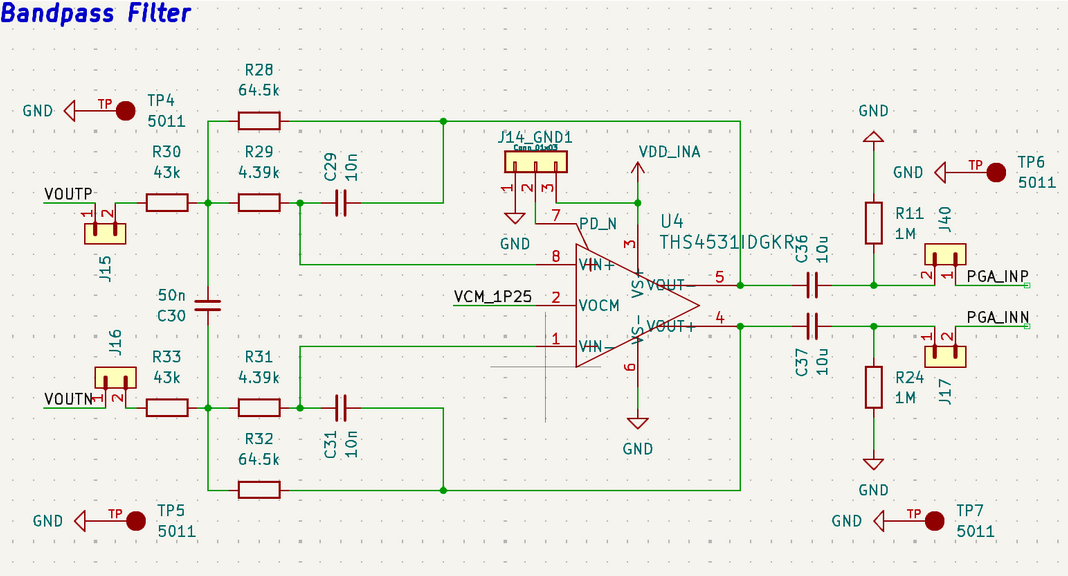
Fig 9. Bandpass Filter Schematic
ADC INPUT INTERFACE
A similar low-pass filter topology is used as an anti-aliasing filter for the ADC input. An RC low-pass filter is also added to prevent kickback issues.
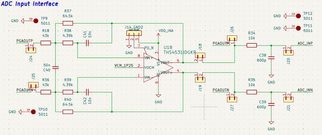
Fig 10. ADC Input Interface Schematic
RIGHT LEG DRIVE CIRCUIT
The right leg drive circuit is very important in the ECG measuring process. We used a commercial opamp to build a CMFB circuit to ensure the human body has the same common mode voltage as the on-chip INA.
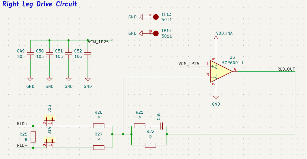
Fig 11. Right Leg Drive Circuit Schematic
OPEN-DRAIN SWITCH
Open drain switches are used to control the 2-bit gain of PGA. Without the jumper, the output node is set to high by default.
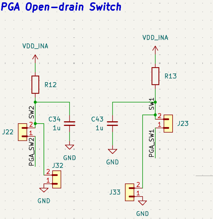
Fig 12. Open-drian Switch Schematic
3.5mm Input Interface
The other ends of the three electrodes are connected to a 3.5mm audio plug, which is then inserted into a jack on the PCB to receive signals from the three electrodes. Series resistors are used for safety considerations.
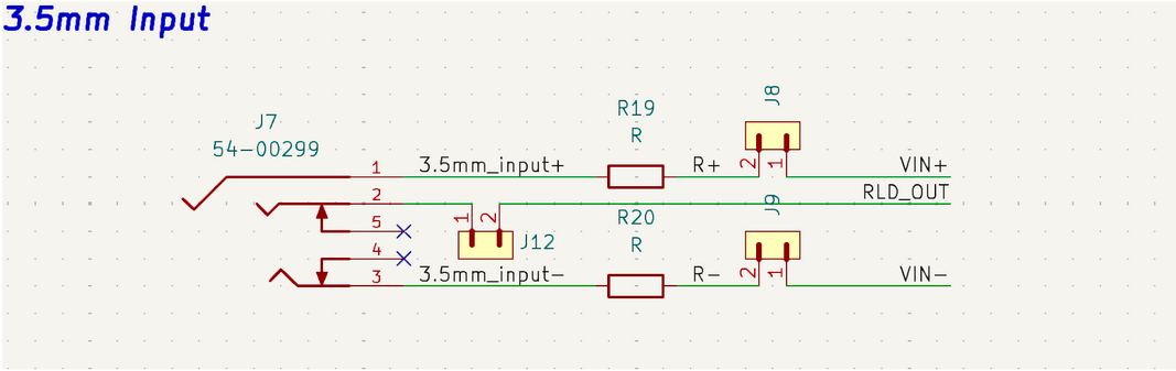
Fig 13. 3.5mm Input Interface Schematic