
Testing
This page documents the testing results, including the overall system functionality check and the performance of each block.
System Level Testing Results
From the demo video on the home page, the receiver is working functionally correct and the whole system can receive the AM channels from the air, select channels by tuning VCO, and change the volume of the speaker by changing PGA gain. The only blemish is because of the poor matching of the crystal filter which introduce insertion loss in passband and poor attenuation in stopband, we can only listen to several strong channels but not all channels.
Performance Results of Each Blocks
Antenna:
Use LCR meter to test the inductance of the ferrite rod coil of 420uH, and the capacitance range of the tunable capacitor from 30-172pF. Use one more coil to do signal coupling and get the bode plots while tuning the capacitor to get different resonate frequency. One of the bode plots of the antenna frequency response is as below, which is the desired LC low pass response and the Q of this antenna is about 10.
LNA:
The waveforms of the LNA's input and output are shown below. As evident from the waveforms, the LNA achieves a gain of 10, corresponding to 20 dB.
LNA Input and Output Waveform
Mixer:
Large Input Signal Testing:
The mixer was tested by injecting a 500 kHz sine wave signal with Vpp more than 40mVpp into the RF input at the designated testing point and providing a 10.2 MHz square wave signal from the LO. The output signal from the mixer buffer was then measured using an oscilloscope. The measurement results are presented below, demonstrating the mixer's performance under these conditions.
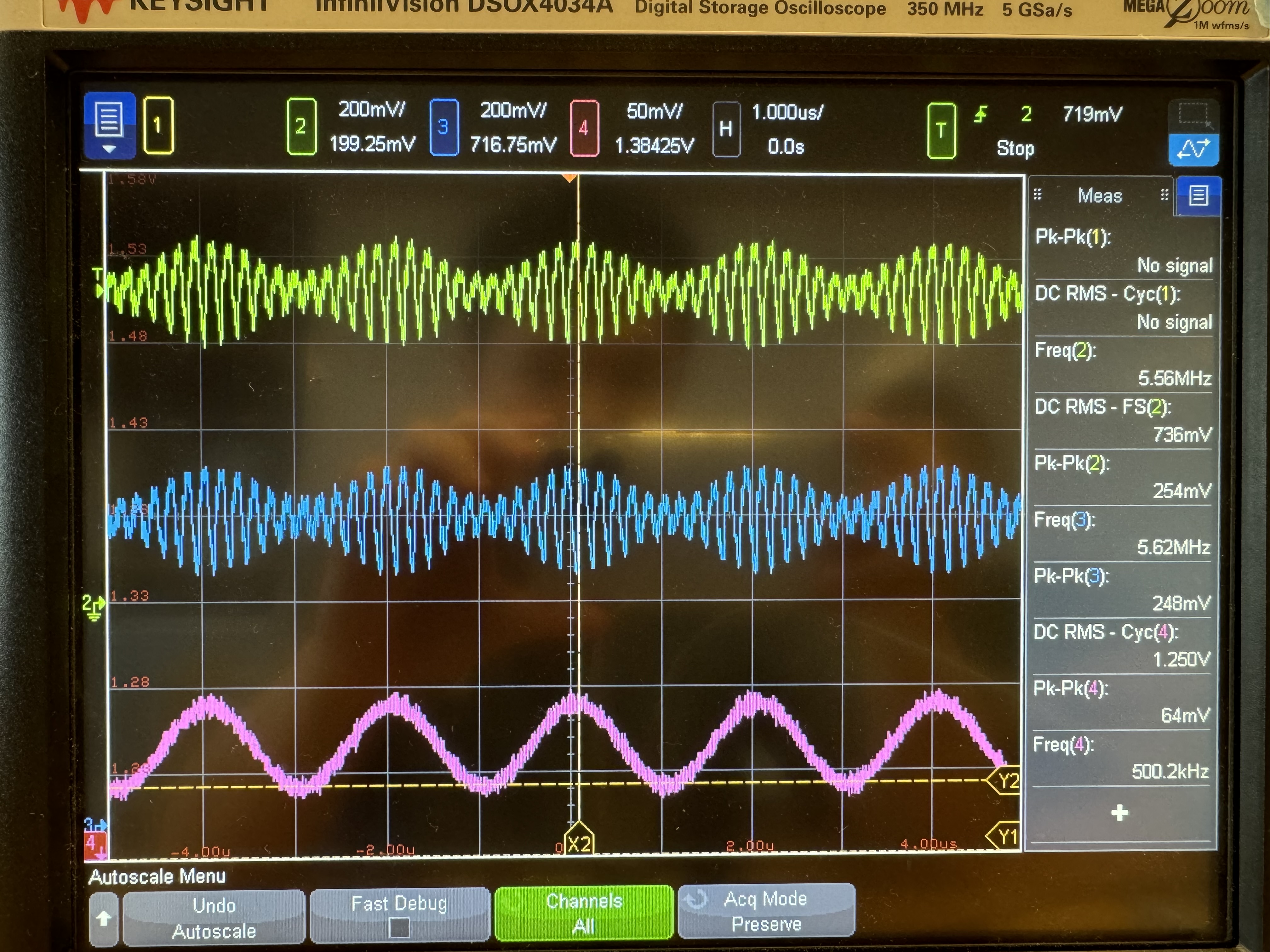
Mixer Output Waveform
Mixer Output FFT Result
However, if the input signal is too large, the signal will make the Mnrf in the mixer to cause nonlinearity. This will cause one side of the output signal to distort,degrading the amplitude and the waveform, as in the figure below.
Distortion in Mixer Output Waveform
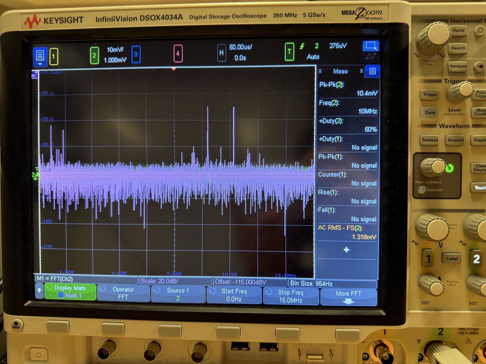
Small Input Signal Testing:
The mixer remains functional when the input signal is small (less than 5 mVpp). However, under these conditions, the waveform is not clearly visible on the oscilloscope. This may be attributed to noise from the probe or wiring. Despite this, the results can still be validated by analyzing the FFT plot, which provides a clearer representation of the signal's frequency components and confirms the mixer's proper operation.
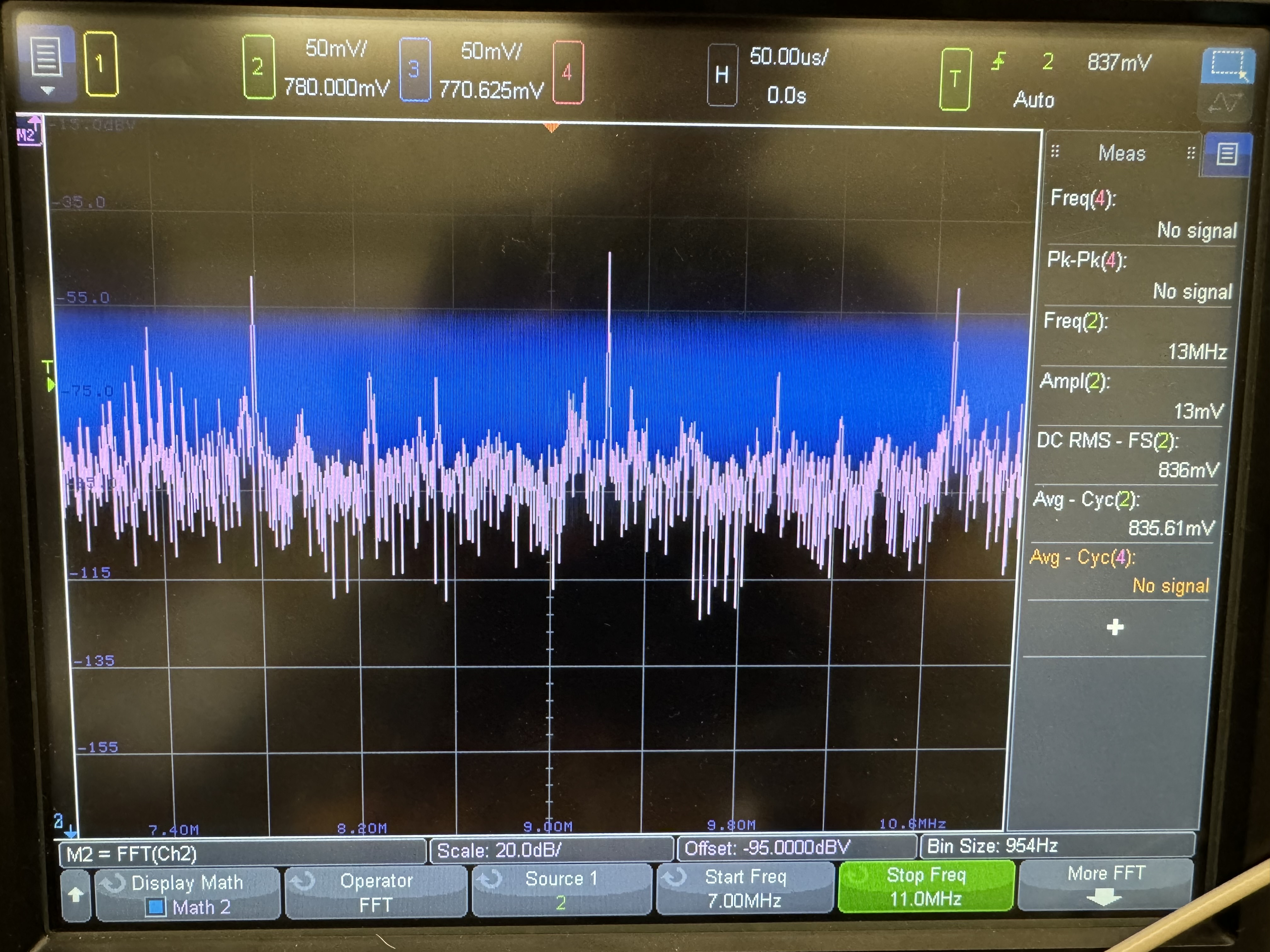
FFT Result with Small Input Signal
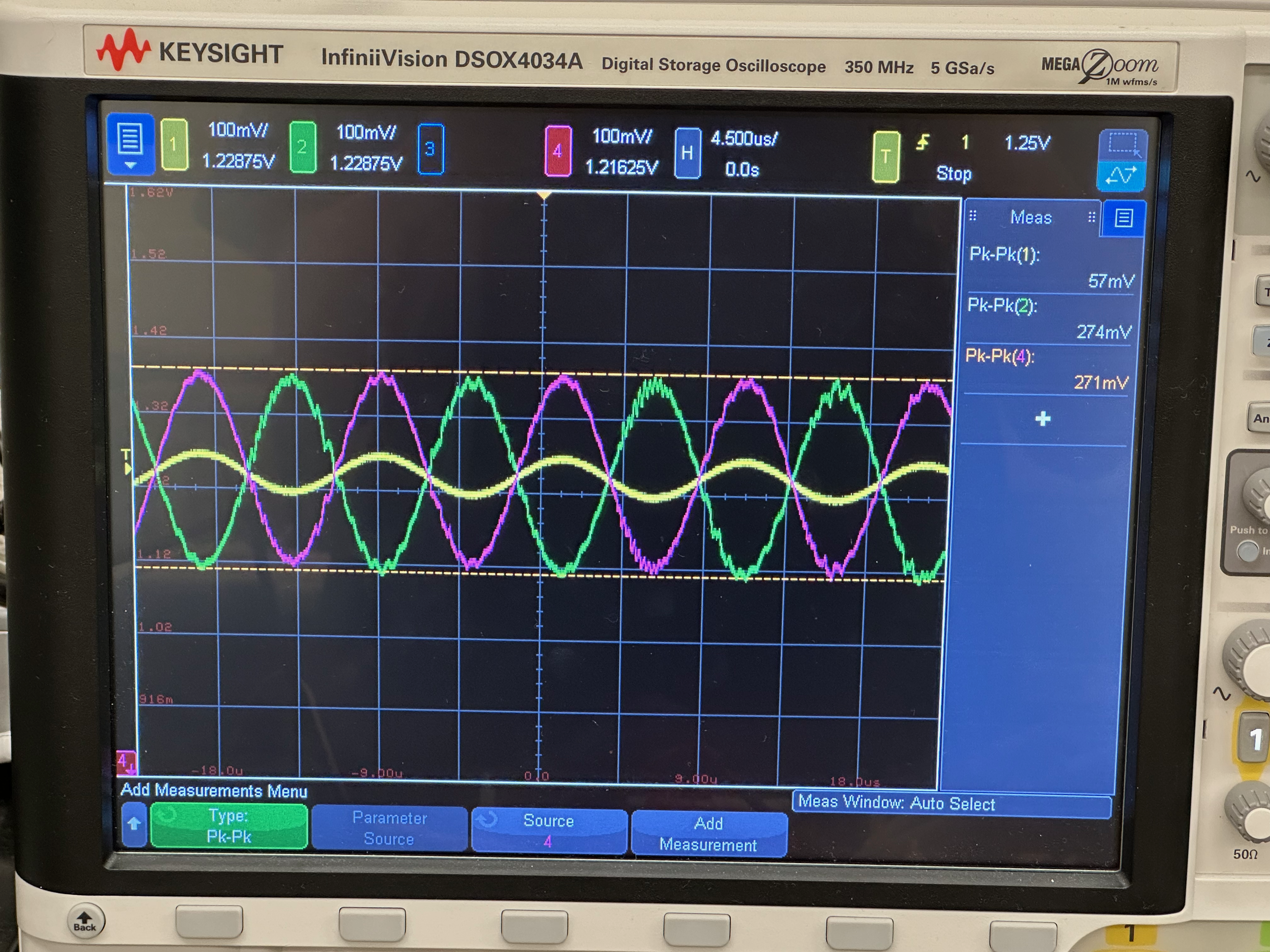
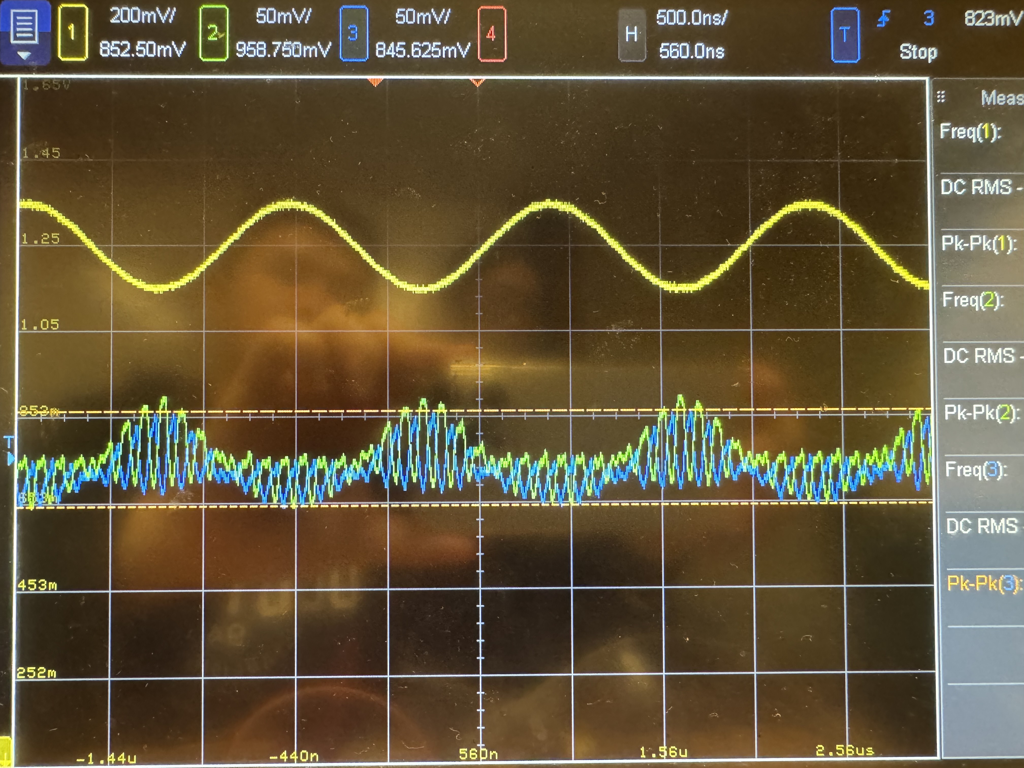
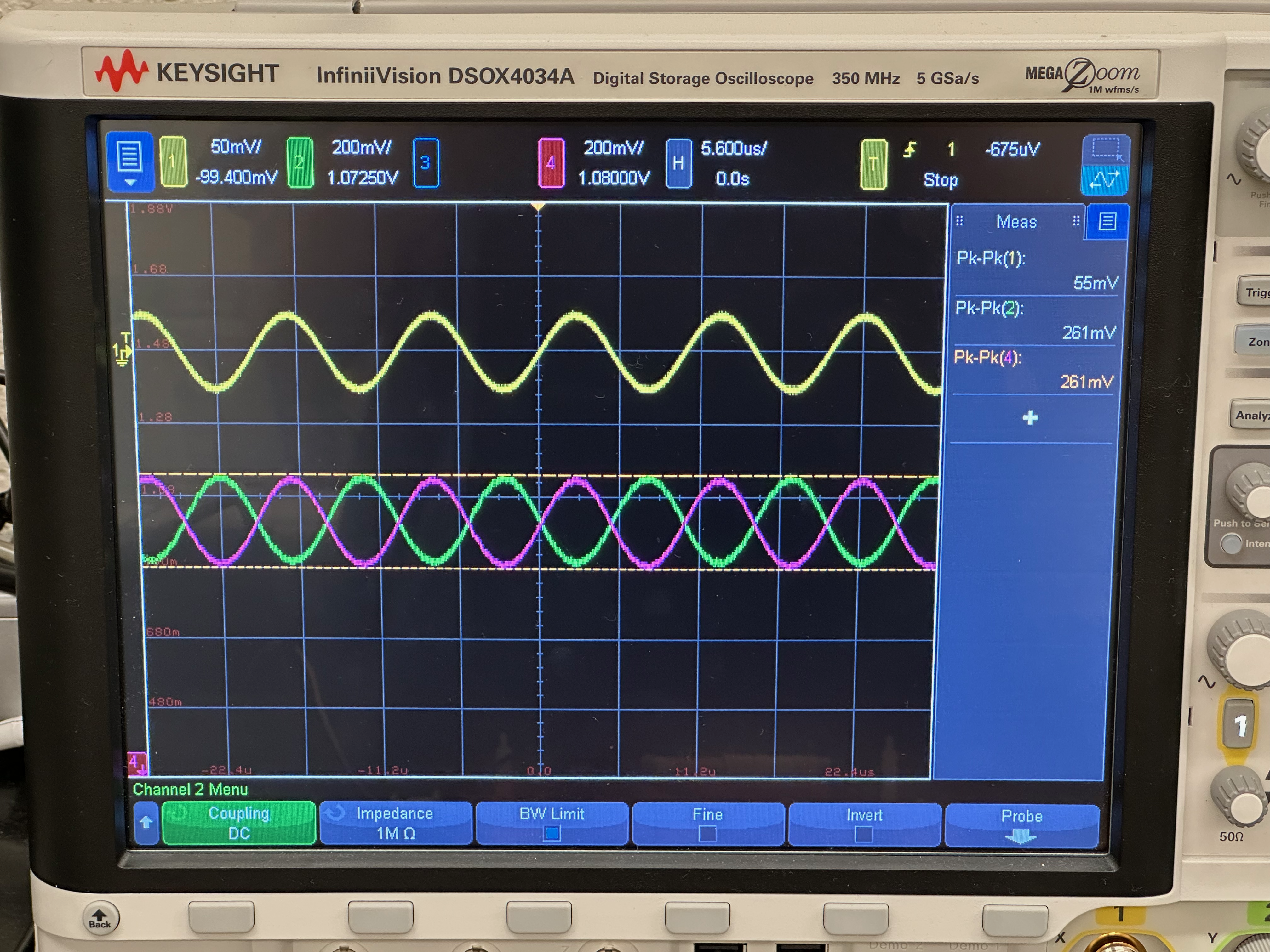
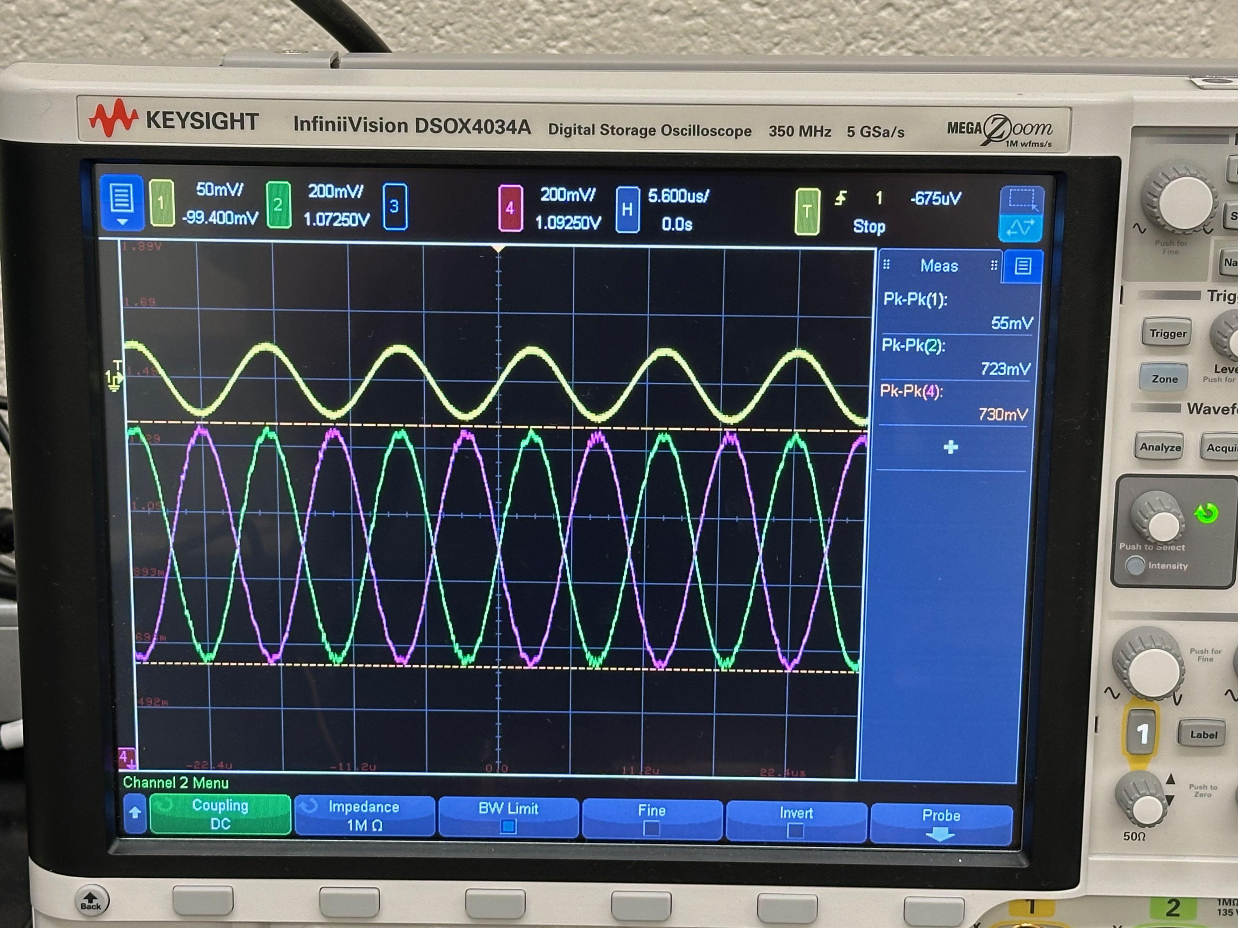
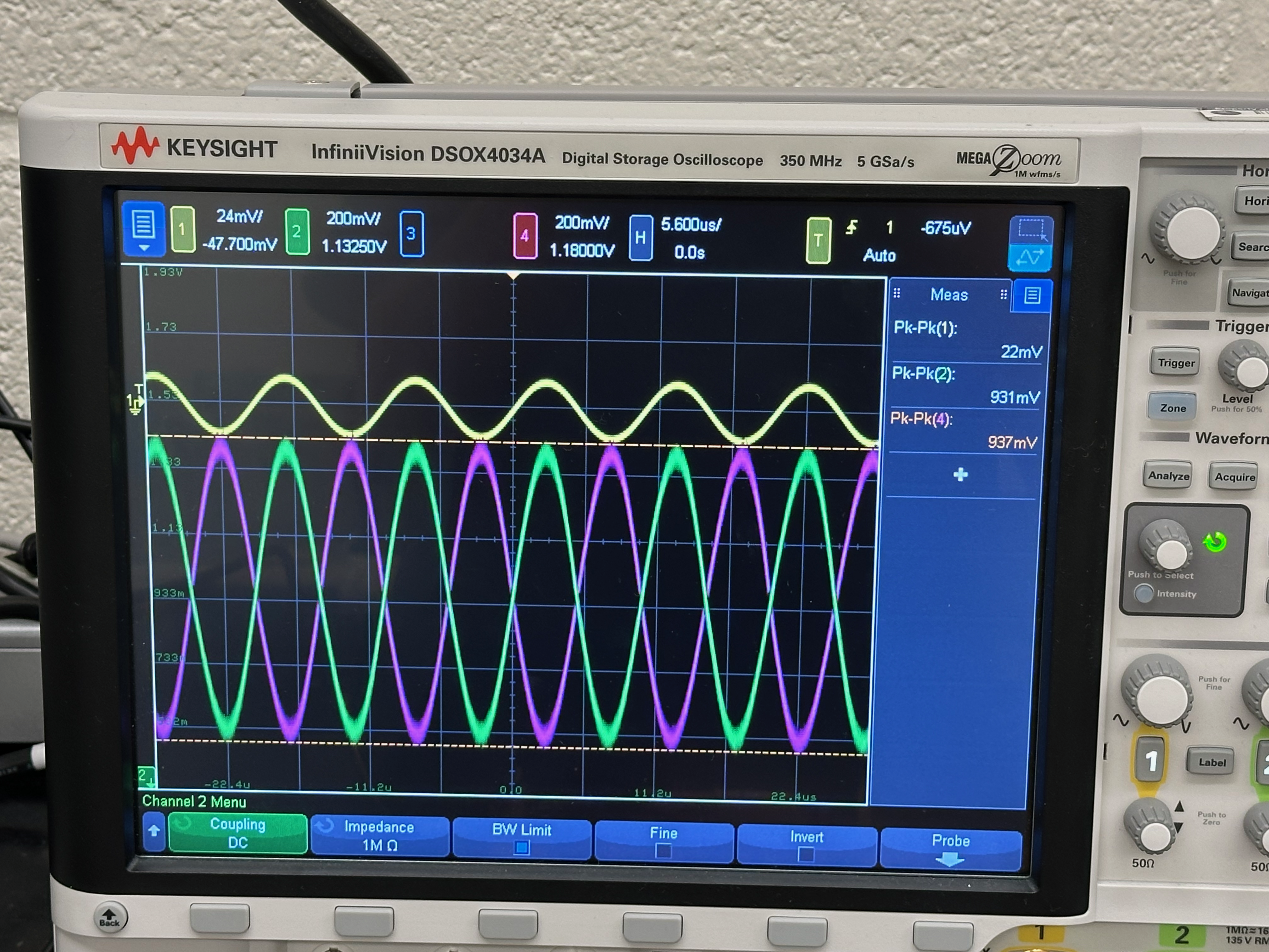
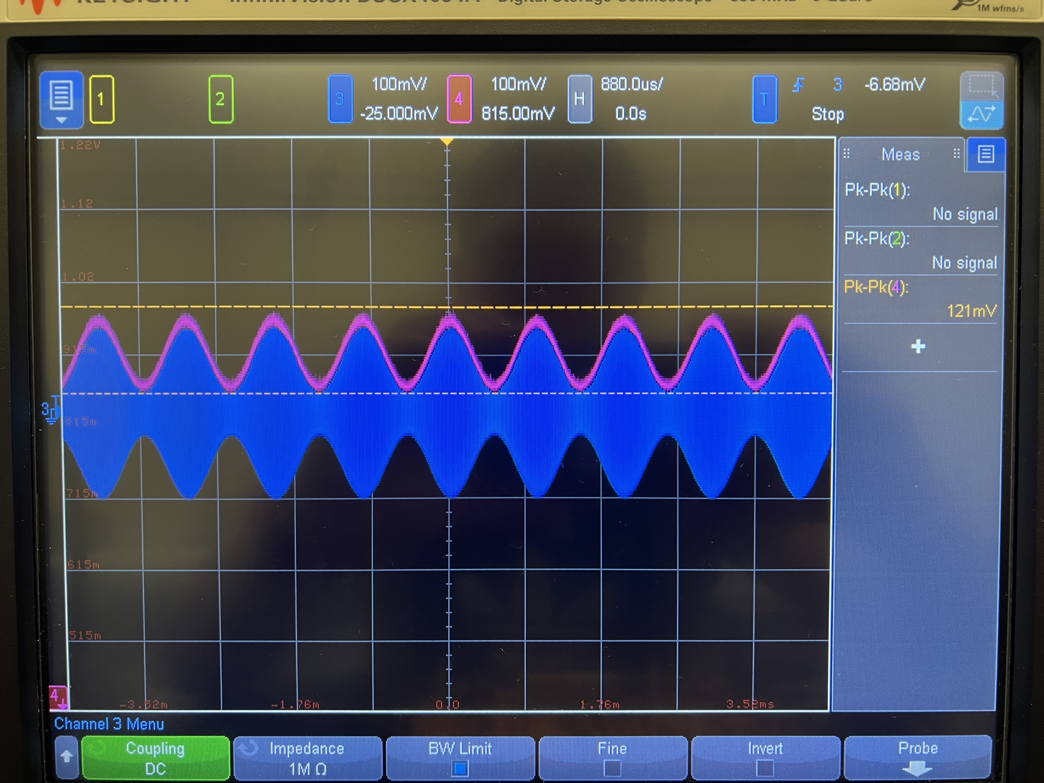
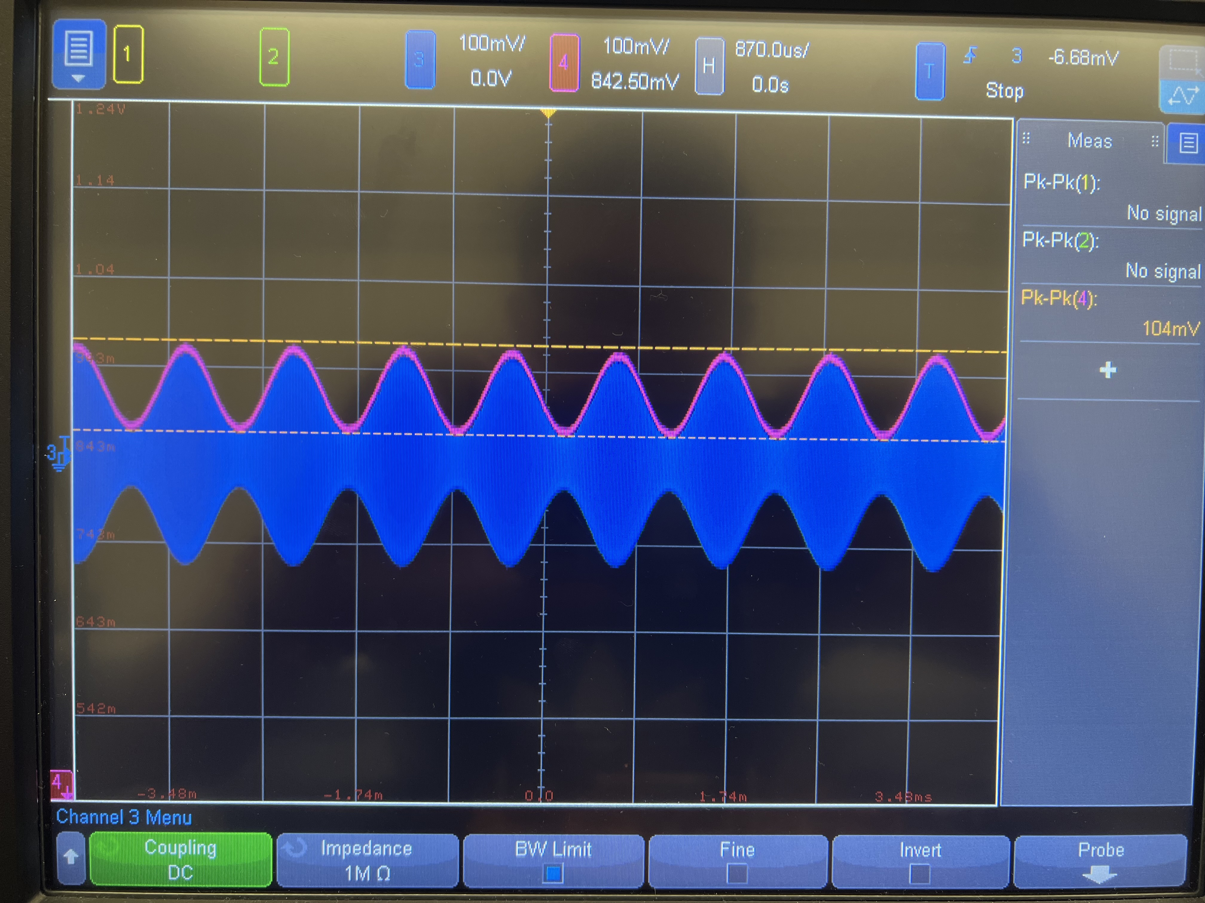
Output DC Bias Voltage :
From the figure below, it can be observed that the envelopes have different peak-to-peak values. This discrepancy arises because the current values in the two buffers are not identical. The likely cause is the difficulty in precisely tuning the potentiometer to achieve the same resistance and value in both buffers. However, this difference in DC bias voltage will be filtered out by the off-chip crystal filter and will not have any significant impact on the overall system performance.
DC Bias Votage Difference in Mixer Output
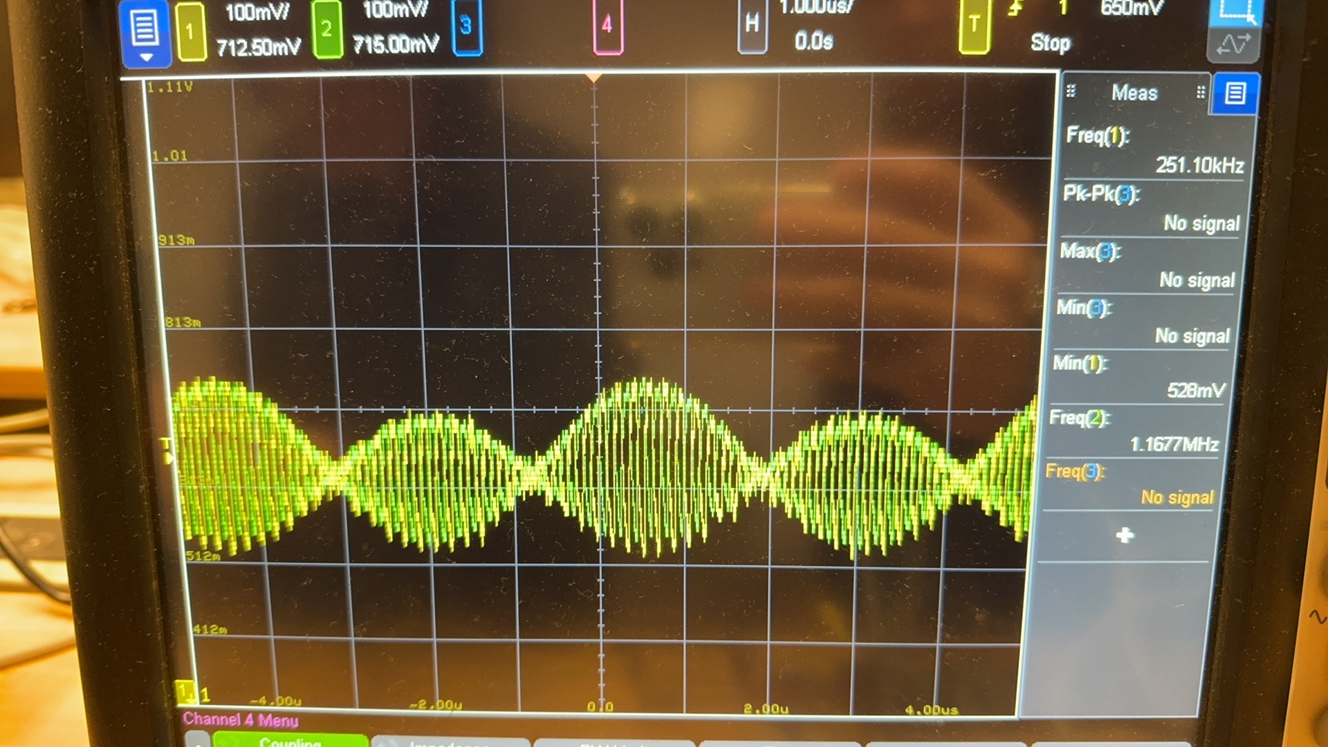
VCO:
Frequency Range and Precision test:
Since VCO only needs frequency from 9 to 10.16MHz, the biasing current for the charge pump is designed to be one fixed resistor that sets the max frequency in series with one small range potentiometer, which achieves tuning from 10.16MHz down to 9MHz.
Choose 25 turns for the small range potentiometer, and about 72deg turn is required for the 10kHz channel step, which means the VCO can be precisely controlled to select channels.
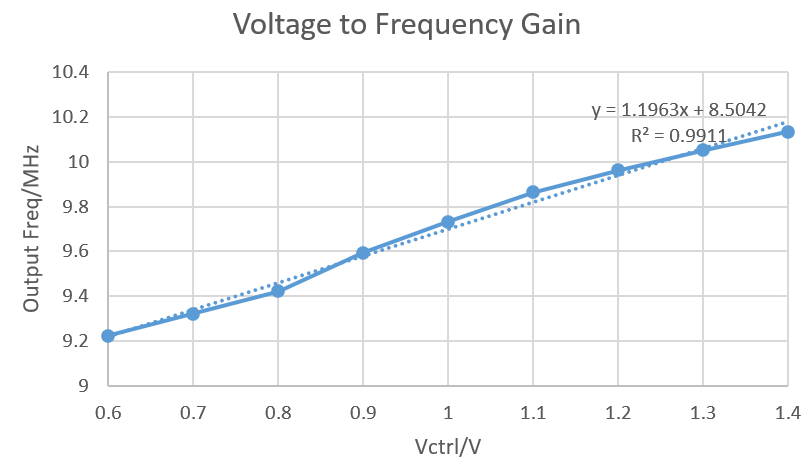
Voltage to Frequency Gain and Linearity test:
Set the VCO to the minimum output frequency of 9MHz and slightly increase the Vctrl for higher frequency. Ignore the voltage lower than 0.6V(where the Vgs is smaller than Vth); the voltage to frequency gain is 1.20MHz/V with a linearity of R2=0.991, and an 8.4mV voltage step is required for the 10kHz channel step, which is also feasible to do 10kHz channel selection.
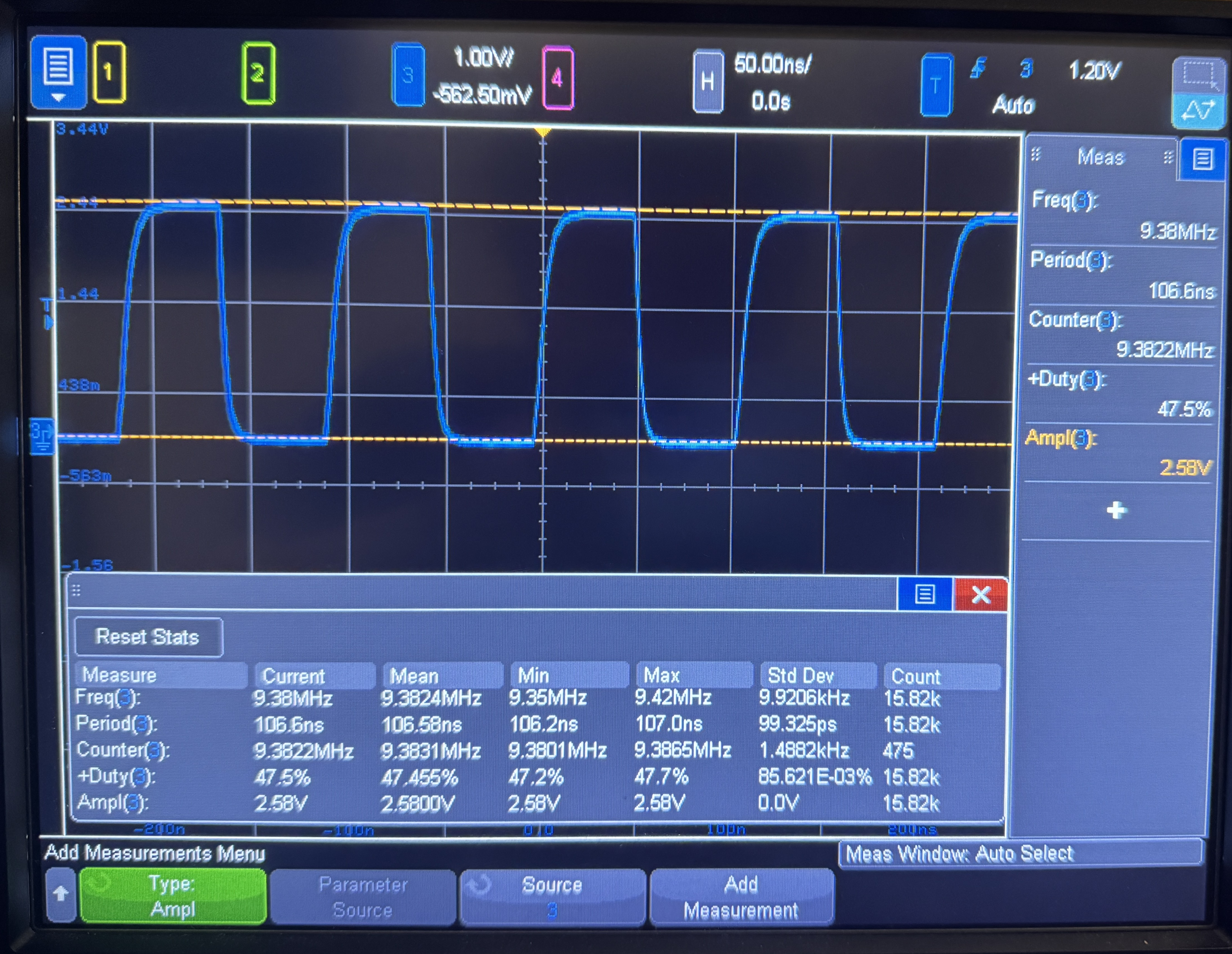
Jitter test:
Integrate the phase noise in the frequency domain gives jitter in the time domain. Use the statistics function of the oscilloscope to sample 15.82k points, and the standard deviation of the period is 99.3ps, which is even smaller than the result in the simulator. This also indirectly shows phase noise is lower than the simulation, which already meets the requirement.
The reason why the edge of the waveform is not sharp is because the loading from the probe is 10pF, which is relatively large enough to flatten out the rising and falling edge.
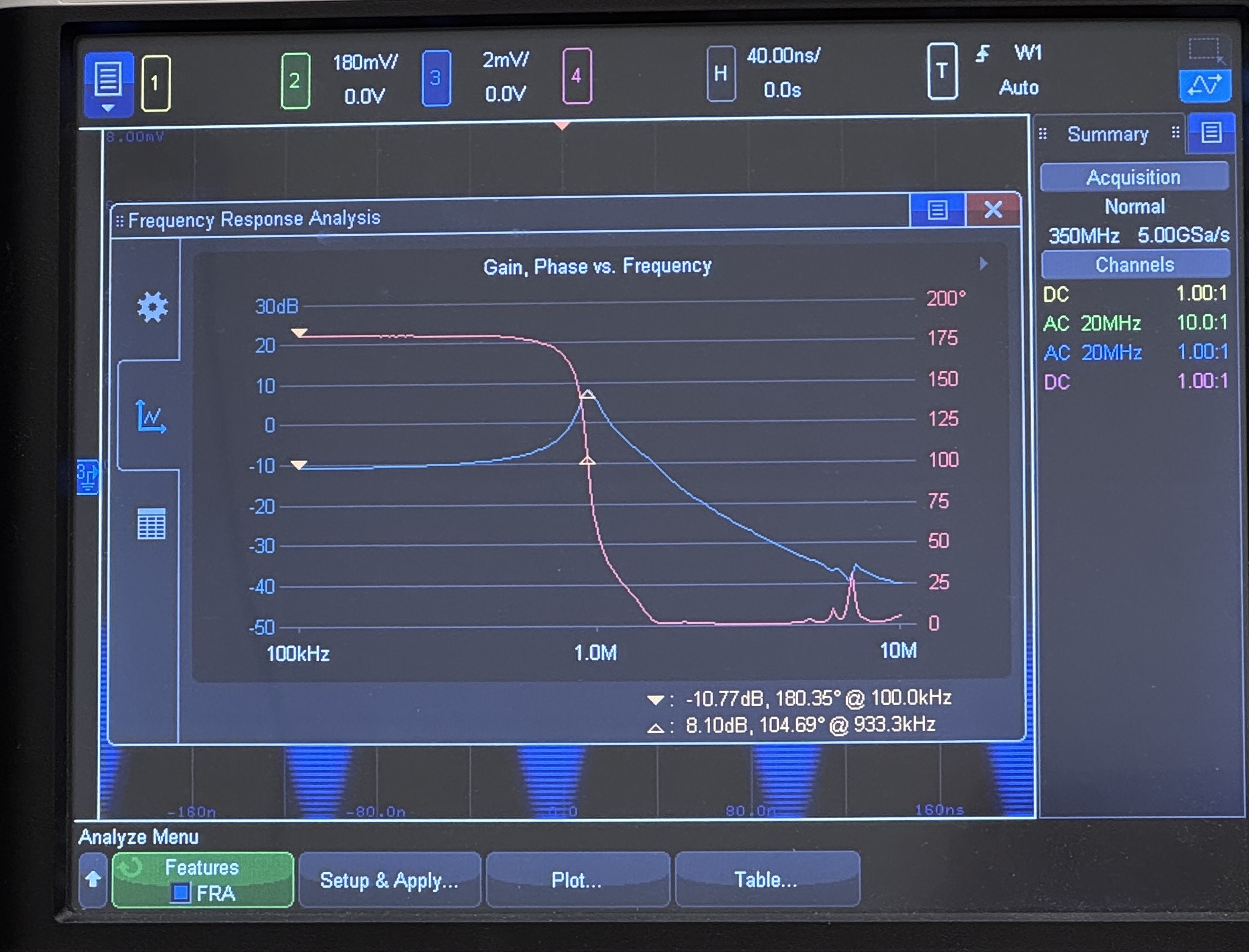
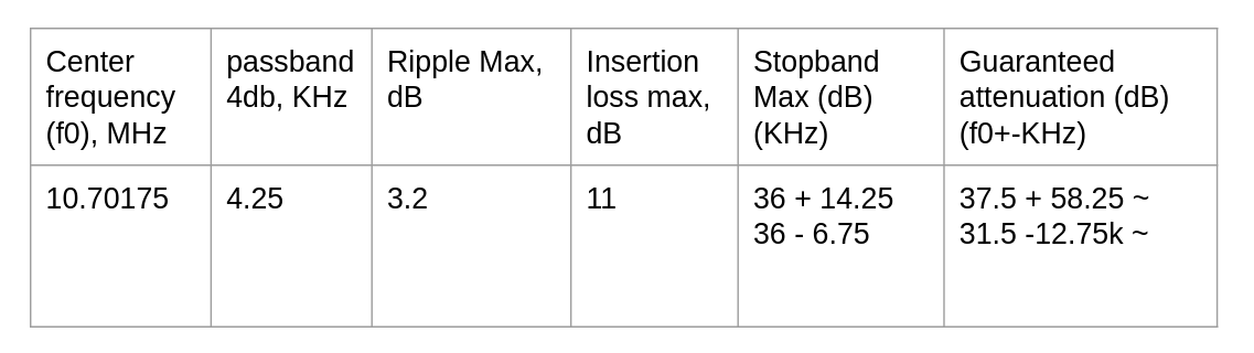
Crystal Filter:
We tested the crystal filter on an empty PCB board using the specified impedance values provided in the datasheet. According to the datasheet, the resistance is 3KOm and the capacitance is 2pF.
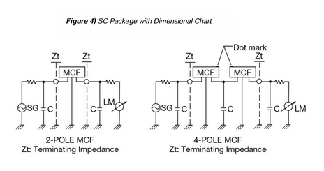
Crystal Filter Test Circuit
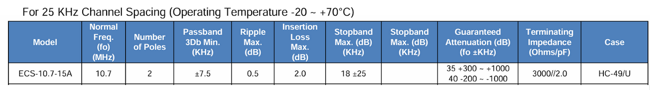
Crystal Filter Specification Table
However, the measured attenuation plot over frequency deviates significantly from the datasheet's specifications. The insertion loss is notably higher than expected, which raises concerns about the potential loss of the targeted frequency signal. Additionally, the out-of-band attenuation is insufficient to adequately suppress unwanted signals.
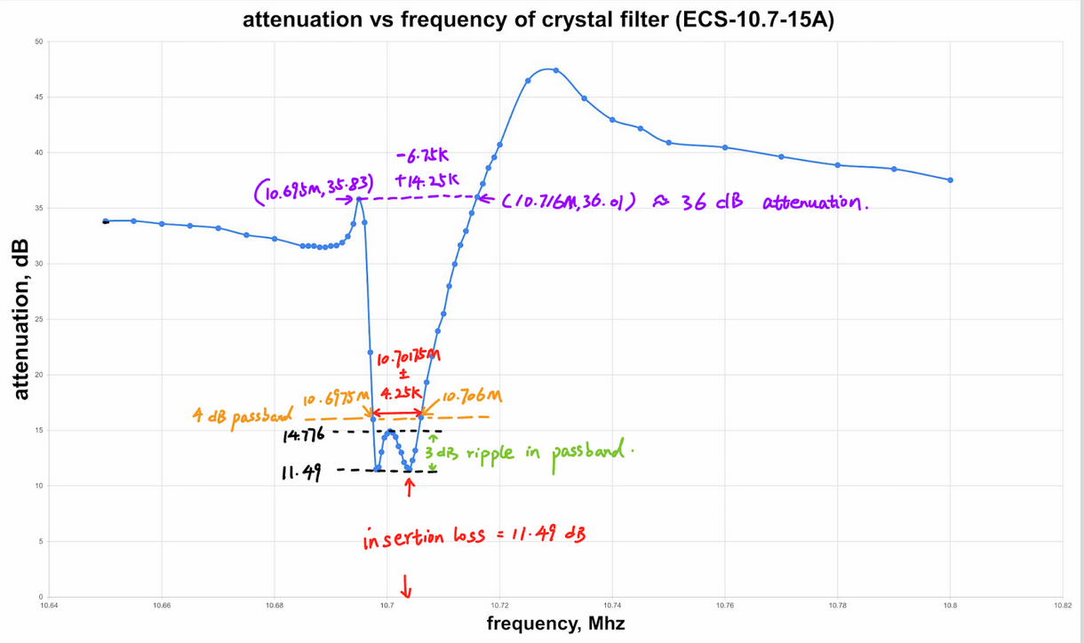
Measured Bode Plot of Crystal Filter
Measured Crystal Filter Specification Table
PGA:
The oscilloscope is unable to display signals with extremely small amplitudes, which prevents testing the PGA with an input small enough to activate all four stages simultaneously. Instead, each stage of the PGA was tested individually to ensure proper functionality. The input and output waveforms for gain settings of 20 dB, 30 dB, and 40 dB are shown below, clear demonstrating that each stage achieves the correct gain.
PGA Input and Output with A Gain of 20 dB, 30 dB, 40 dB
Demodulator:
Output at the envelop detector
Output at the sallen-key low-pass filter