
IC Design
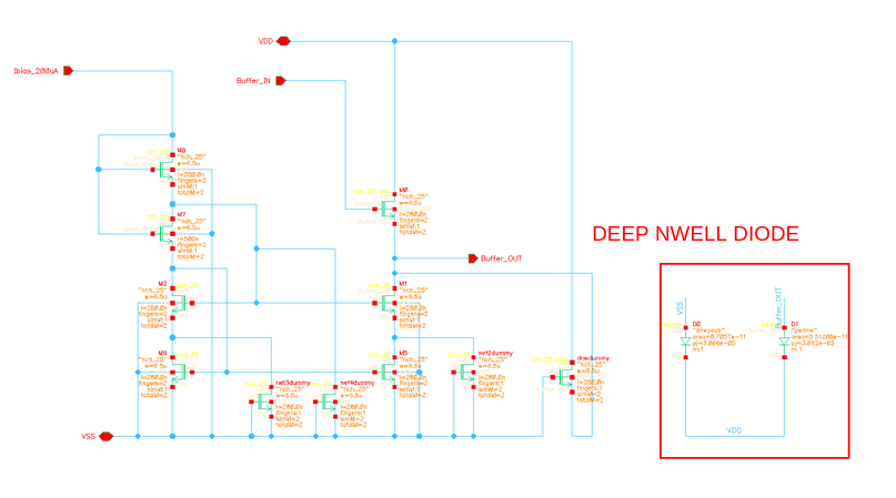
This page includes the detailed transistor-level IC design. The top-level (Cadence) schematic of the receiver is shown below. We have five main blocks on chip, and through signal chains, we introduce LNA, Mixer, LO, GPA, and Demodulator.
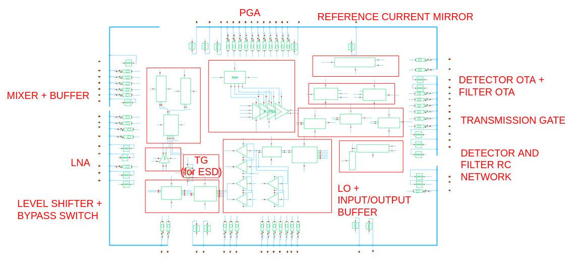
Chip schematic
Low Noise Amplifier (LNA):
LNA design
The primary function of the LNA is to amplify the weak incoming signal from the antenna while introducing minimal noise to the system. The LNA utilizes a cascode amplifier configuration, consisting of a common-source input stage driving a common-gate output stage. It employs a resistive load, which, while reducing the gain, improves the output noise performance compared to active load topologies. Additionally, a common-mode load resistor is applied at the LNA’s output to establish the common-mode level of the output signal, which biases the RF port of the mixer, without overly increasing the gain prior to any filtering or channel selection. The LNA block diagram is shown below. <\p>
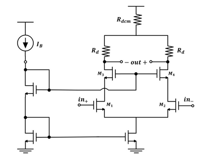
LNA Architecture
The gain of the LNA is determined by Rd, with a resistive load chosen instead of a cascode load because the gain provided by Rd was deemed sufficient. The cascode topology was primarily selected to block IF signals coupling back from the mixer, thereby preventing interference with the amplification transistor pair and enhancing input-output isolation. At the AM input frequencies of operation, the flicker noise contributed by the differential pair transistors plays a critical role. To minimize this noise, the transistors were designed with longer channel lengths and correspondingly wider widths, ensuring the desired performance was achieved.
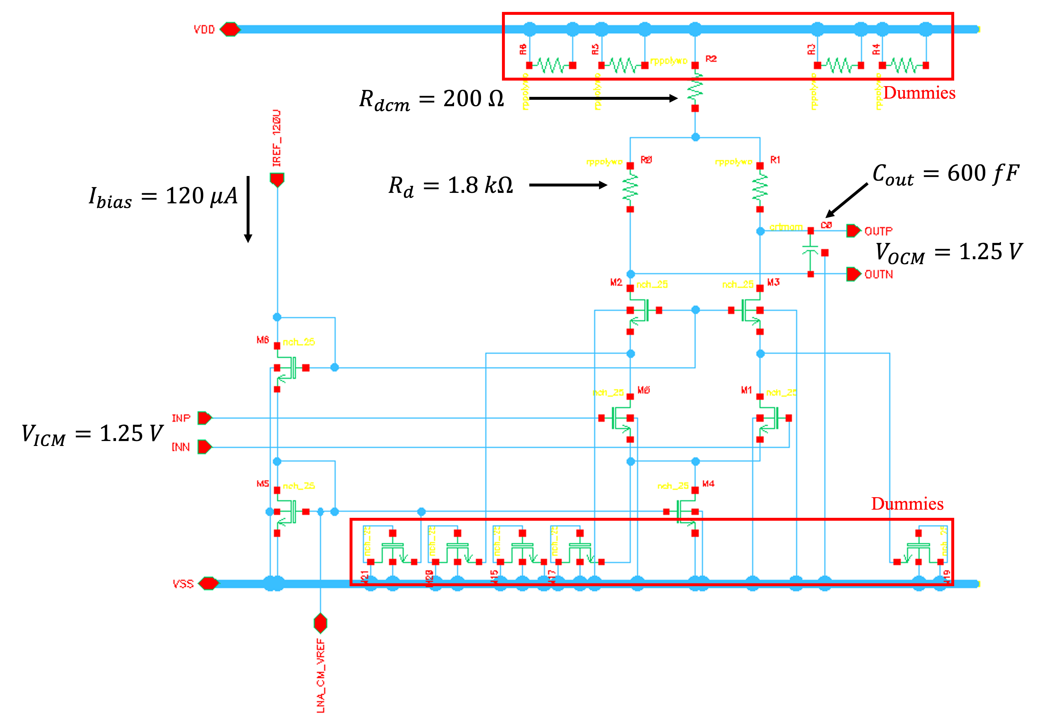
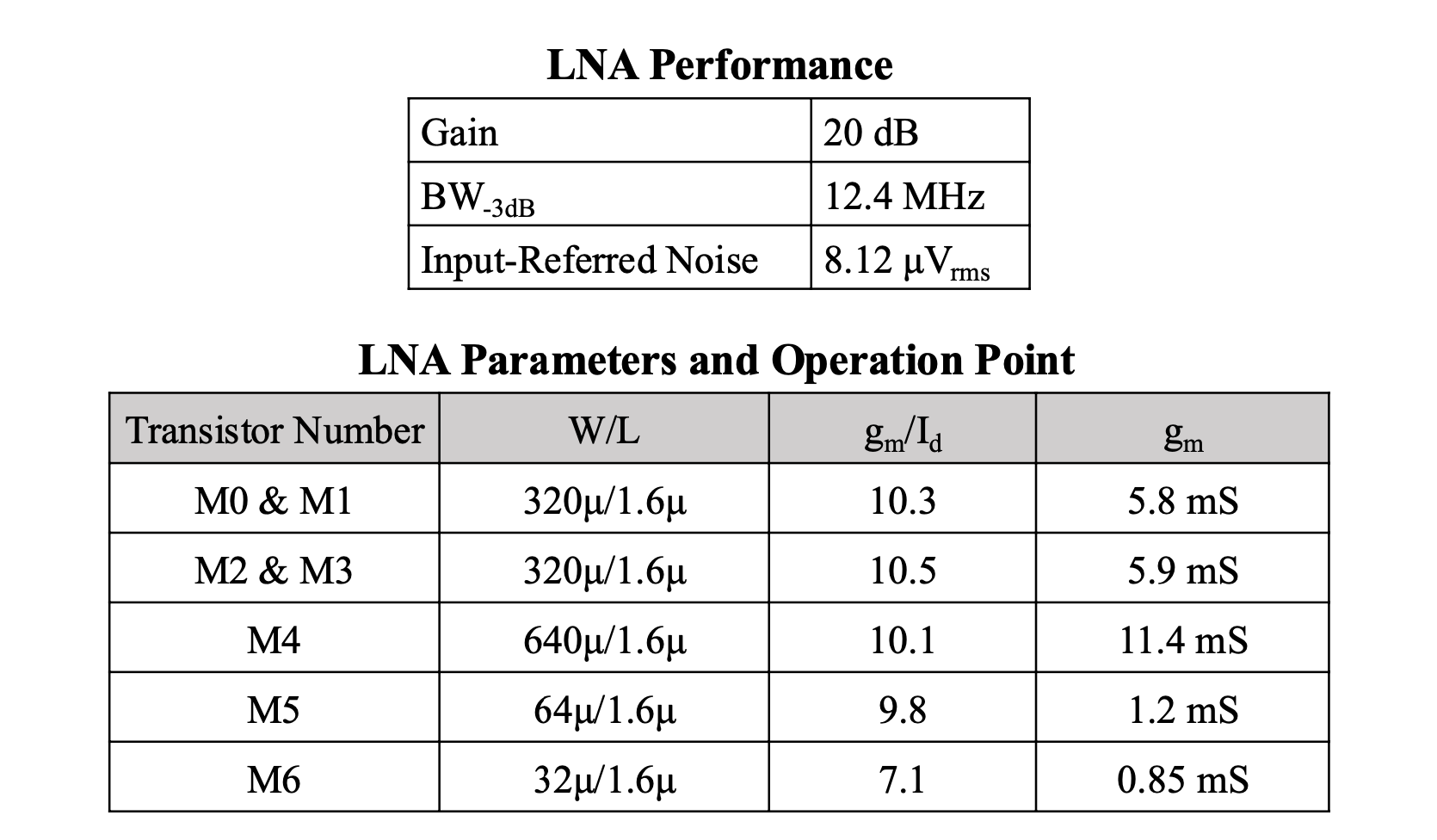
LNA Schematic and Specification Table
LNA Frequency Response and Input-Outout Waveform
Mixer:
The mixer is designed to perform frequency up-conversion from the desired AM channel to an intermediate frequency (IF) of 10.7 MHz. It features two differential input ports: one for the RF signal and the other for the LO signal. The design prioritized linearity and conversion gain to address the insertion loss in the off-chip crystal filter, ensuring minimal loss of the target RF signal during the up-conversion process. The schematic architecture of the mixer is illustrated below.
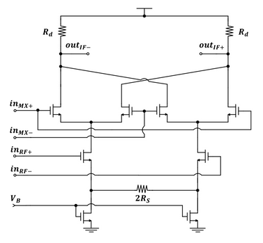
Mixer Schematic Architecture
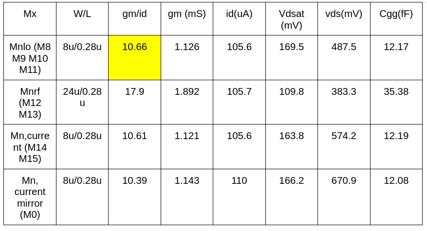
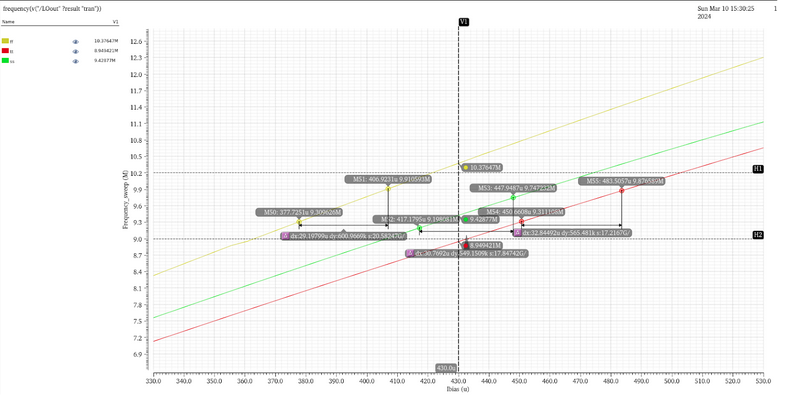
The Cadence schematic and the design specifications tables are presented below. At first, we set Mnlo to have a large gm/id that has a similar behavior to a switch. Yet, we found out that a lower gm/id will have fewer spikes while maintaining the behavior of a switch. Thus, as highlighted in yellow, the gm/id ratio of the transistors for the LO input is designed to be 10. This specific design choice helps to mitigate more significant spikes in the transient response during rapid switching of the transistors. The dc bias for Mnlo is 1.5V with an amplitude of 250 mV. The Conversion Gain of the mixer is 3.18x, with a BW of 31.393MHz.
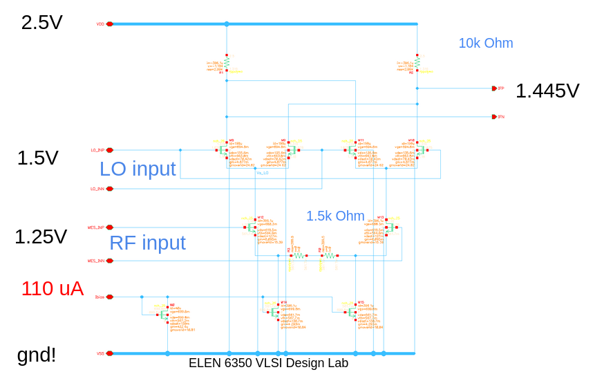
Mixer Schematic and Specification Table
The mixer's performance was thoroughly evaluated through simulations conducted in Cadence.
On the top side of the simulation results, the RF input signal is shown as a 4 kHz message signal modulated onto a 1.311 MHz carrier, mimicking the AM signal received by the antenna and amplified by the LNA. Additionally, a 9.389 MHz signal generated by the LO is presented.
The resulting product of the 1.311 MHz RF input signal and the 9.389 MHz LO signal is displayed on the bottom side. The presence of spikes in the output is attributed to the parasitic capacitance between the input and output.
Mixer Simulation Waveform
Mixer Buffer:
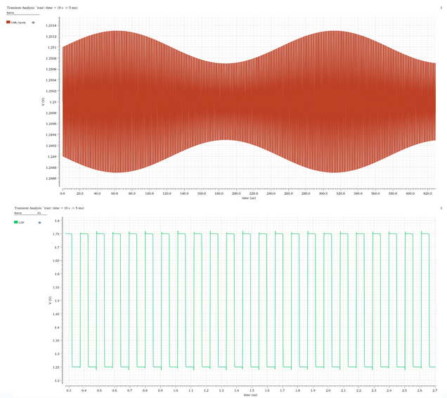
The buffer is implemented as a cascoded source follower, designed to interface the output of the mixer with the input of the off-chip crystal filter. This architecture ensures proper impedance matching and isolation, reducing loading effects on the mixer. The sehmetaic and spcification table are shown below.
Mixer Buffer Schematic and Specification Table
The output resistance of the mixer buffer is 500 Ω, and its gain is 0.95x. The gmbs of M0 is 265μ, which is significantly larger than the sCL (134μ) at 10.7 MHz. This ensures the circuit does not exhibit negative resistance, avoiding any potential instability or oscillation issues. This careful design consideration enhances the overall reliability and performance of the mixer buffer.
Voltage-controlled oscillator(VCO):
As introduced in previous pages, the local oscillator in this system should be frequency tunable(voltage-controlled or current-controlled) and can cover frequencies from 9-10.16MHz, and the tuning precision should be at least 10kHz. Ring oscillators are hard to do precise frequency control, and LC tank oscillator frequenciey is hard to go down to 10MHz, so this design chooses the relaxation oscillator, and the block diagram of it is below:
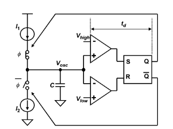
VCO block diagram
How It Works:
1. Suppose at the beginning Vosc is 0V: the lower comparator output "high"; the Reset port activated; Qb is "high"; current source I1 charge the Cap(switch active low); Vosc linearly increase.
2. Vosc becomes higher than Vhigh: the upper comparator output "high"; the Set port activated; Q is "high"; current source I2 discharges the Cap(switch active low); Vosc linearly decreases.
3. Vosc becomes a triangle wave, and each time it is higher than Vhigh or lower than Vlow, Q, and Qb as the square wave outputs flipped.
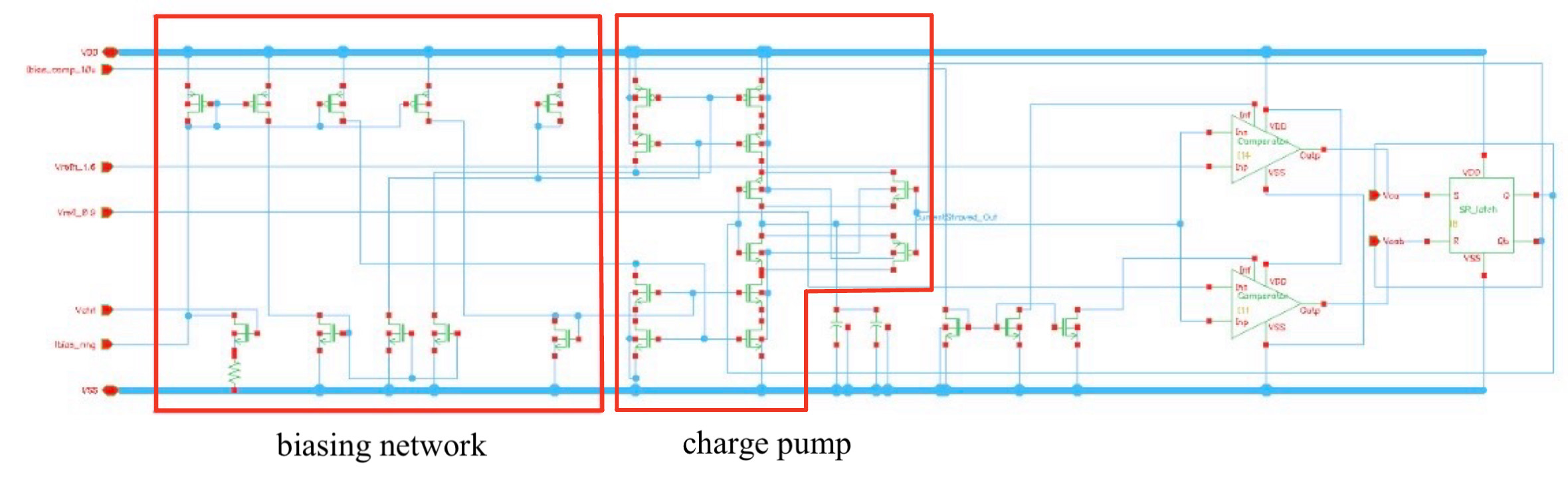
Charge pump design:
The Vosc swing is the larger, the better(will be discussed later), so Vds of the diode-connected simple current mirror will change a lot, making current copying imperfect, so current mirrors using wide swing cascode design to shield the Vds effect.
Also, to minimize charge injection when switching, the PMOS and NMOS of the transmission gates are sized in the same (W/L) and minimal L.
The way to realize frequency tuning is to change the current of the charge pump to make it charge or discharge the capacitor faster or slower. There are two ways to realize this:
- 1) Use a source degeneration common source as a voltage-controlled current source to realize voltage control.
- 2) Use a potentiometer but not a fixed resistor to directly generate the tunable bias current.
VCO charge pump transistor level
Comparator Design:
Two comparators are using the following topology. The reason why not to use a simple opamp is because the internal positive feedback in this comparator makes it respond faster. Suppose (W/L) of M15: M14= M16: M17= a. To make the comparator latching(positive feedback), choose a>1. The comparing speed is highly dependent on the Vov of PMOS, so this design made them 200mV. Hysteresis is strongly related to the Vov of NMOS differential pair and a, so make NMOS Vov 72mV and a=2 to minimize hysteresis.
Obviously, comparator output can only go to VDD-Vgs, and can not go down to VSS, so one skewed inverter as output buffer is essential.
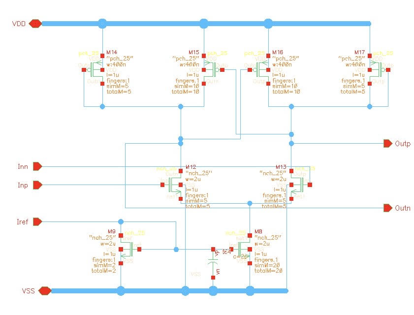
VCO comparator transistor level
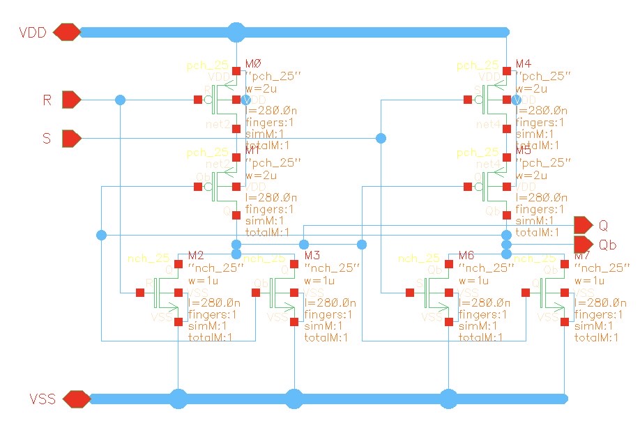
SR Latch and Level Shifter(Driver)Design:
Use NOR-based SR latch and transistor sizing is based on FO4. The mixer can't accept rail-to-rail square wave clock input, so it is necessary to level shift the LO signal to 1.25V and 1.75V using an analog multiplexer.
VCO SR latch and VCO driver
Design Phase Noise Optimization:
Phase noise is a critical target in every oscillator design because it is how jitter appears in the frequency domain. The worst case in this system is the target channel signal is the weakest (50uV), and the strongest signal (5mV) is just 10kHz next to it, so there is a 40dBc difference. To avoid the influence of this strong signal, at least -60dBc/Hz at 10kHz offset phase noise is expected.
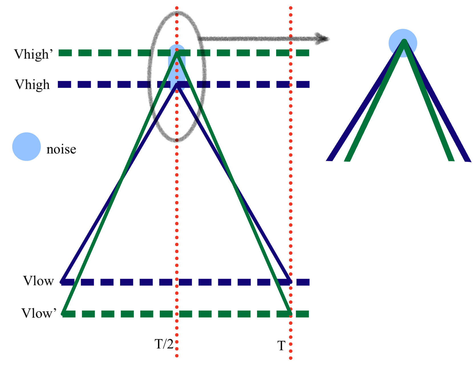
To simplify analysis, only focuses on the most sensitive point (when Vosc is equal to Vlow or Vhigh and start to flipping):
- 1) To achieve the same frequency, the larger the Vosc swing, the higher the slope of the Vosc, and the shorter the time to flip (see picture below).
- 2) The shorter the comparing time, the shorter the time to flip, so that's why a fast comparator is required.
- 3) Noise on Vosc is kT/C noise so the larger the capacitance the smaller the noise.
Therefore, to achieve better phase noise, the tradeoff is to have larger capactor, and larger current from charge pump, which burns more power, and design the current mirrors can just hold the large Vosc swing and limited maxmium output to 10.2MHz.
VCO phase noise optimization
Simulation results are the following:
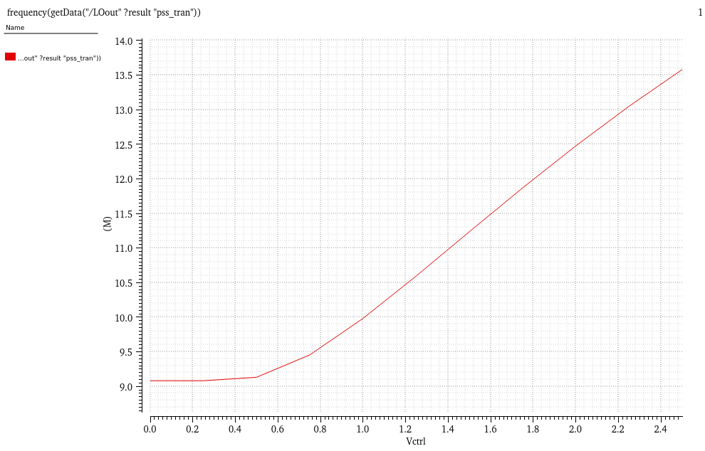
transit results of Vosc, LO out and LO Driver out on the left, and voltage control frequency gain simulation on the right:
PVT simulation of current to frequency gain on the left and phase noise simulation on the right. Integrate the phase noise from 1m to 10kHz gives a jitter of 120ps:
Programmable-Gain Amplifier (PGA):
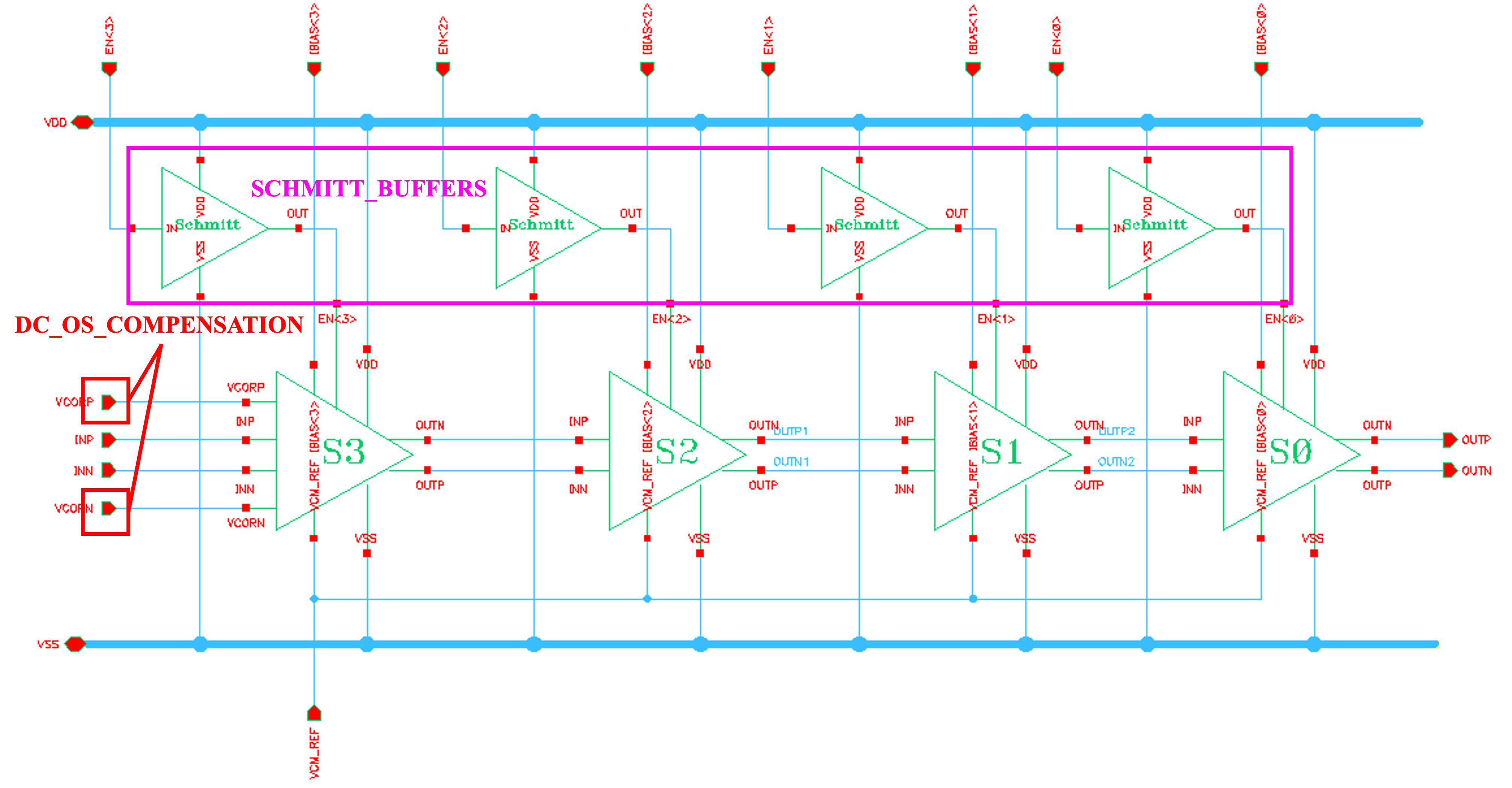
The PGA amplifies the selected AM channel, which has been upconverted to the IF frequency of 10.7 MHz. Variable gain functionality is incorporated to handle a wide range of input signal levels, thereby enhancing the system’s dynamic range. The block diagram of the four-stage amplifier is shown below. It consists of four fully differential closed-loop amplifiers. Variable gain is achieved through differential multiplexers placed after each amplifier stage. The output signal is selected via a combination of four enable bits, enabling gain settings of 10 dB, 20 dB, 30 dB, 40 dB, 50 dB, 60 dB, and 70 dB.
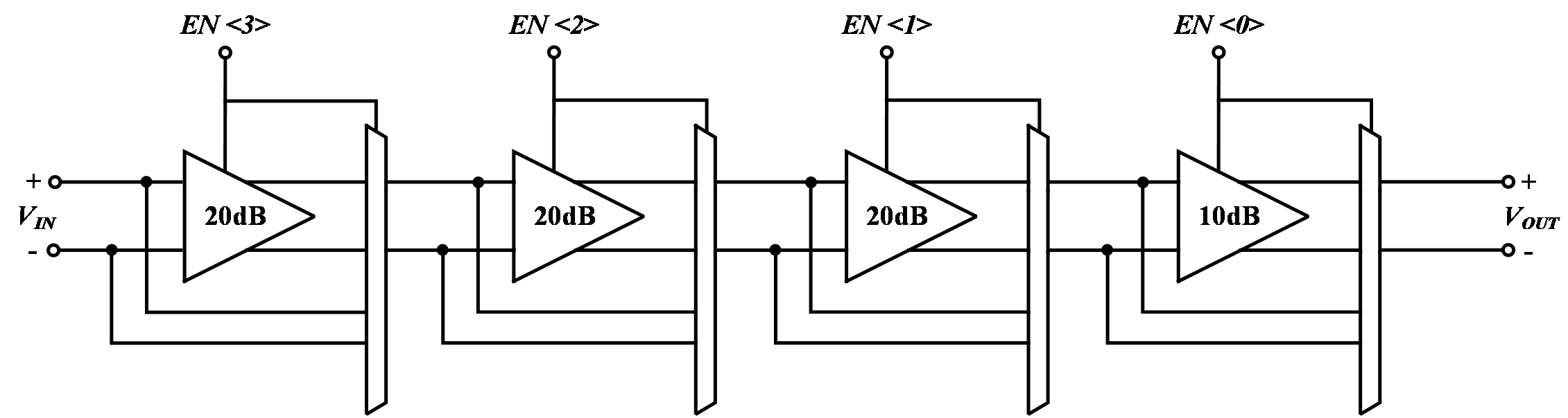
Four-Stage PGA Block Diagram
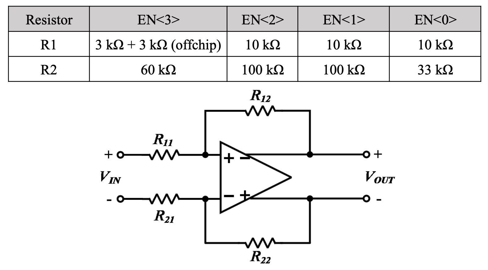
Single-Stage PGA Block Diagram and Resistor Values
The schematic of the PGA is shown below, with multiplexers integrated into each stage. DC offset poses a significant challenge in high-gain systems, as it can accumulate and be amplified through successive stages, potentially leading to serious output issues. To mitigate this, pins VCORP and VCORN are provided for off-chip DC offset compensation. Additionally, Schmitt buffers are implemented to ensure that each stage can be reliably turned on or off, maintaining stable and predictable operation.
Four-Stage PGA Schematic
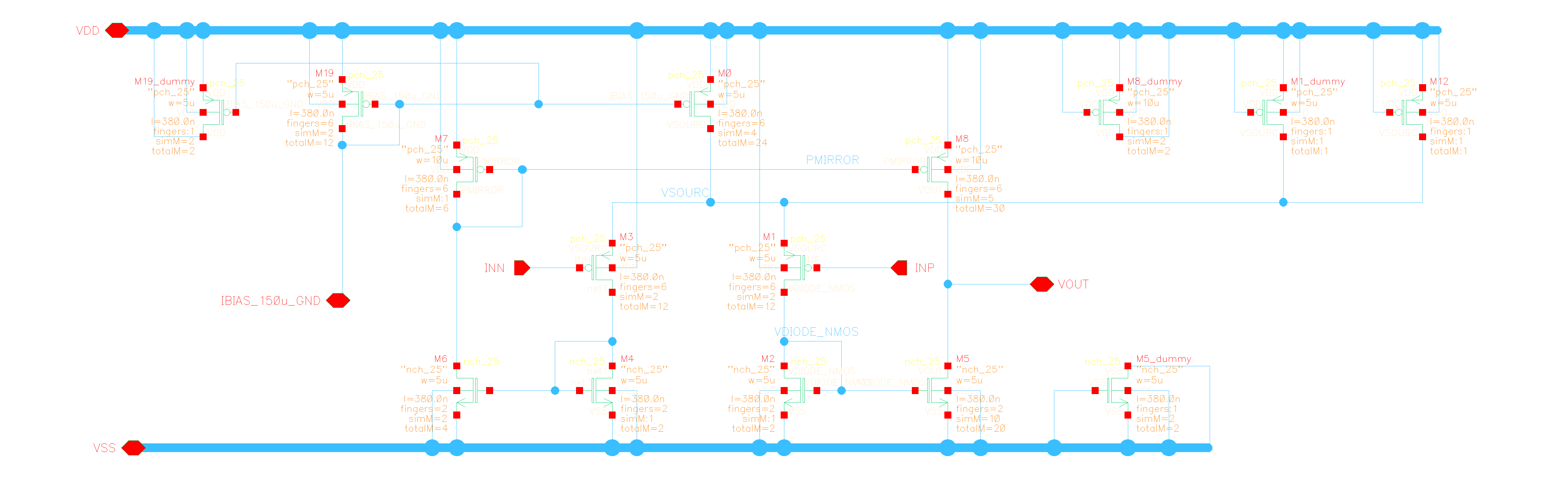
The schematic of the core OTA of a single-stage PGA is shown below. It features a two-stage, fully differential architecture with Miller compensation and integrated common-mode feedback circuitry. The common-mode detector employs a resistor in parallel with a capacitor, with the resistors matched to ensure accurate common-mode output detection. Together with the resistors, the capacitors introduce a zero that cancels the pole created by the common-mode feedback error amplifier. When the enable signal (EN) is logic high, the circuit operates as a standard OTA. Conversely, when EN is logic low, the enable signals activate transistors that pull specific gate voltages to VDD or GND, effectively disabling the OTA.
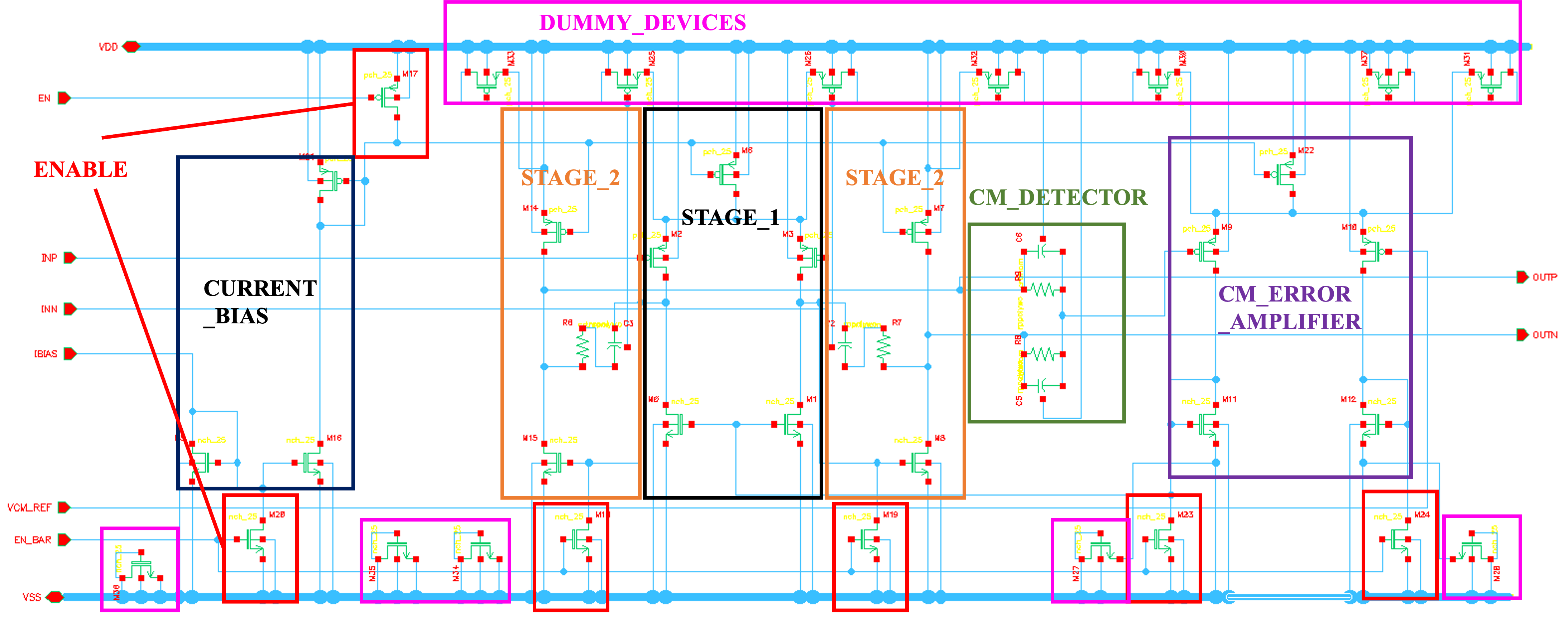
Core OTA of Single Stage PGA Schematic
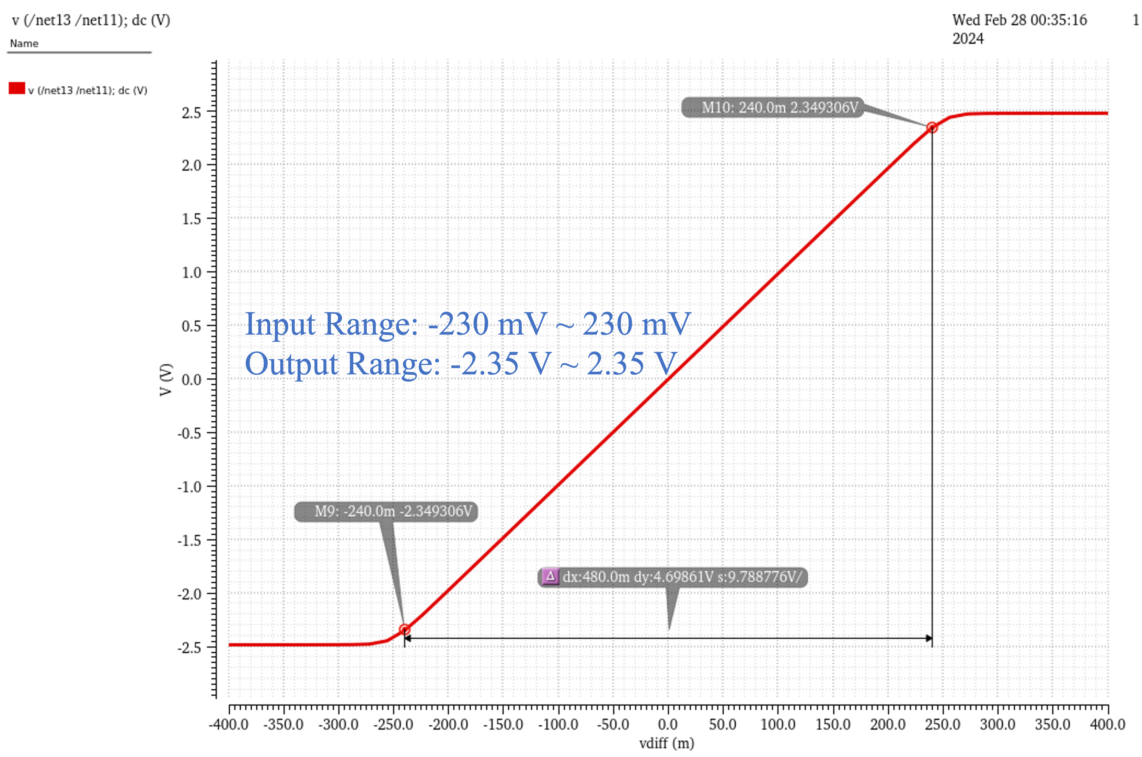
PGA Differential Input Output Range
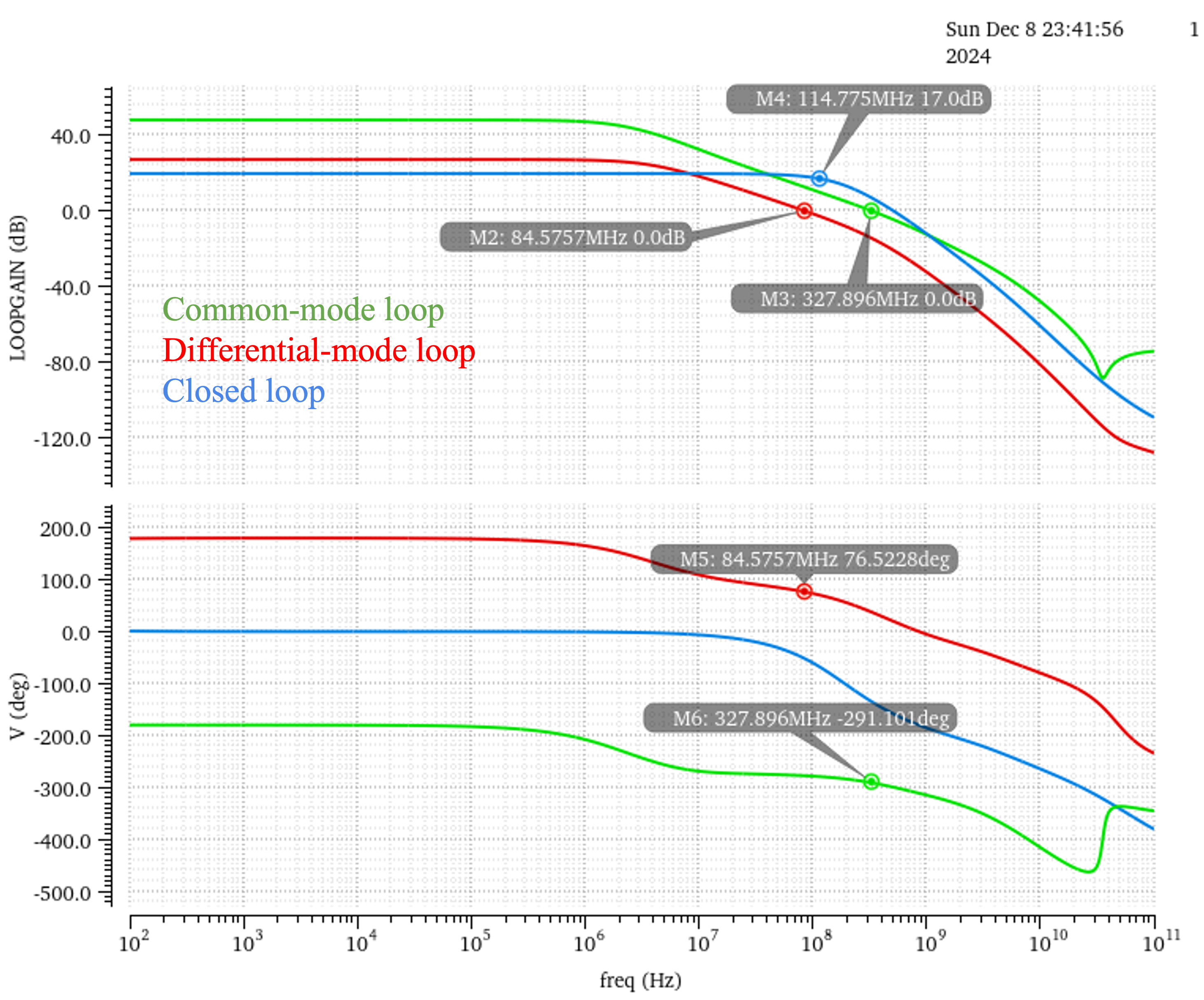
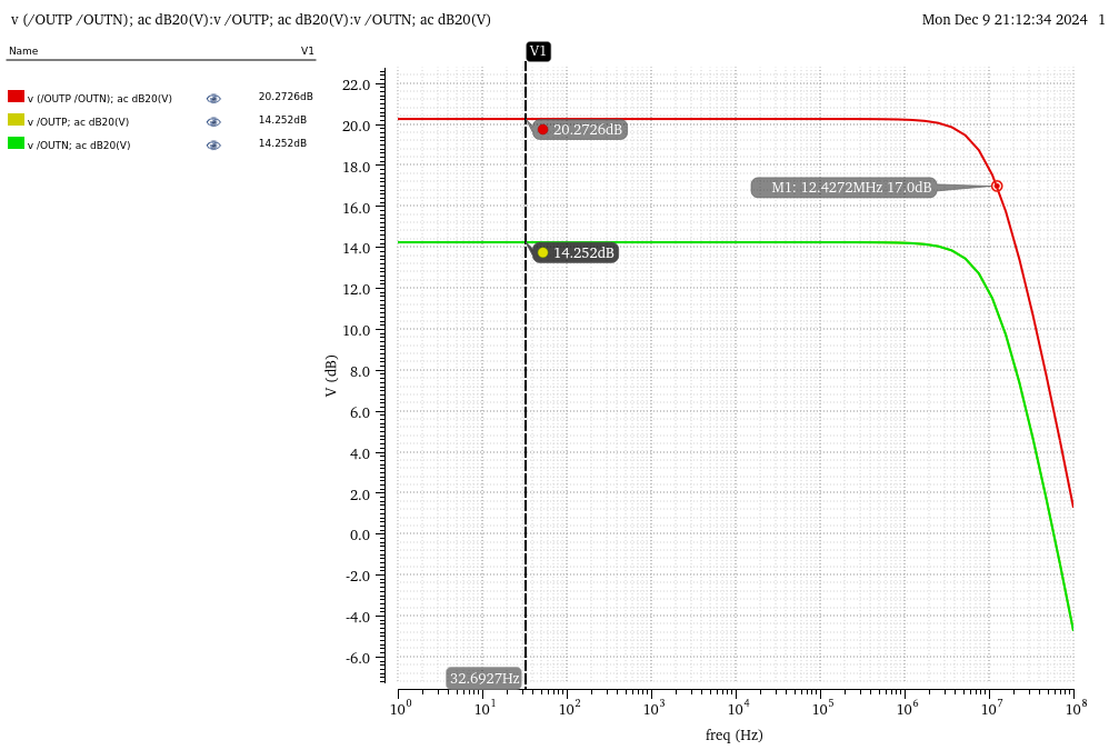
Core OTA of Single Stage PGA Frequency Response
PGA Differential Frequency Response with Heavy Load
Demodulator:
Envelop Detector:
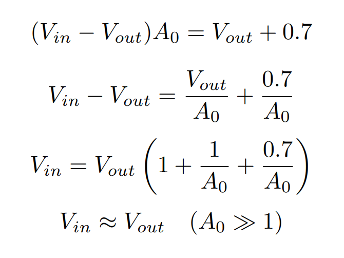
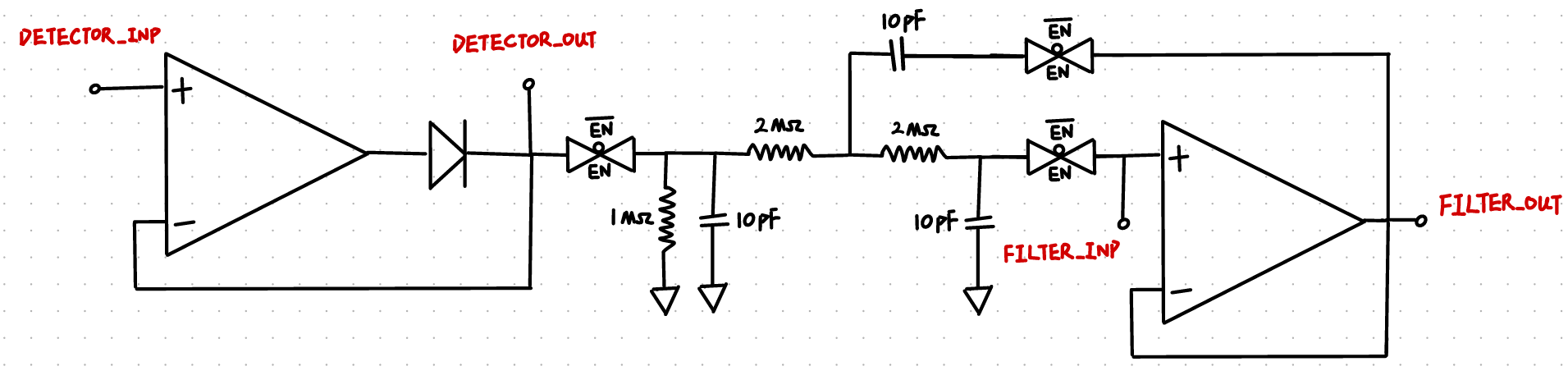
After the PGA (Programmable Gain Amplifier), the amplitude of the 10.7 MHz modulated signal is amplified as expected, ranging from 50 mV to 600 mV. The demodulator tracks the peak of the modulated signal to extract the envelope, which carries the audio information. It utilizes a "super-diode" topology to ensure that the output accurately follows the peak of the modulated signal. This topology integrates an amplifier and a diode to form a "super-diode" structure.
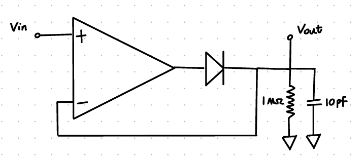
Super-diode block diagram
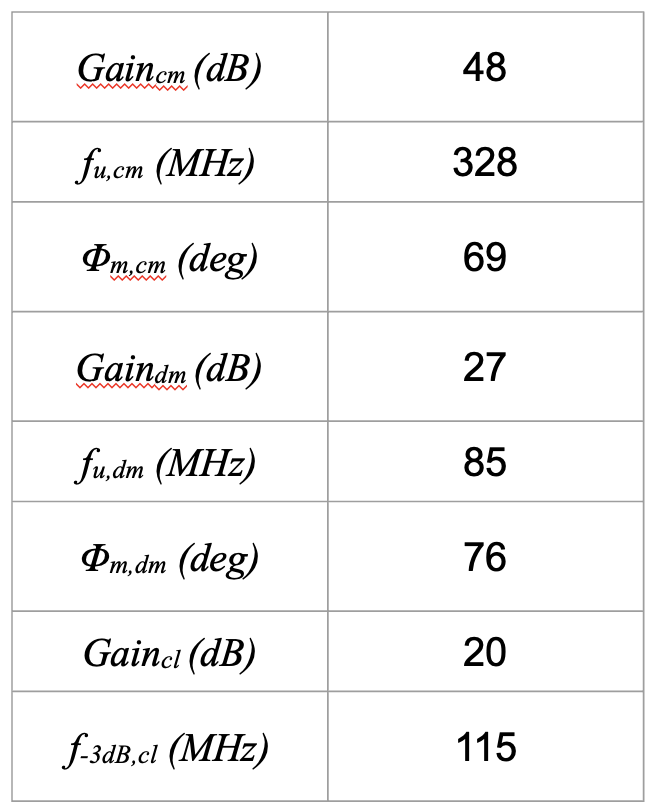
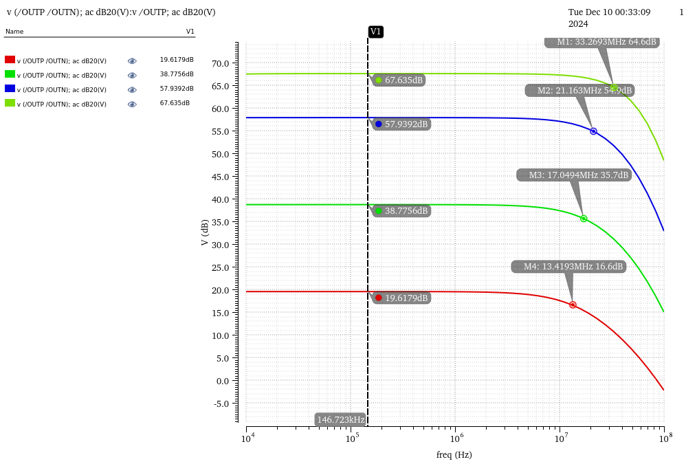
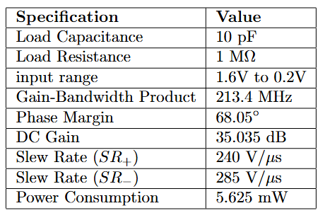
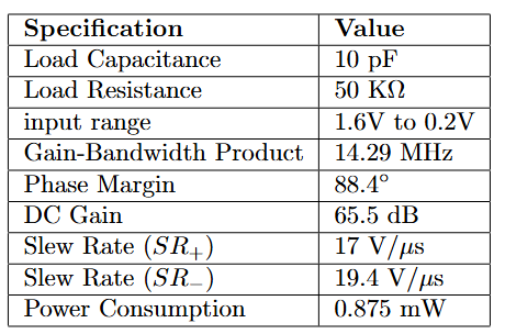
A critical aspect of the design is that the amplifier must have a sufficiently high unity-gain frequency to maintain adequate gain at 10.7 MHz, even under high capacitive loads. This minimizes the voltage drop caused by the diode and ensures precise peak tracking. To achieve this, the detector amplifier adopts a two-stage, non-Miller compensated operational amplifier design. The amplifier provides a gain of 26 dB at 10.7 MHz with a load capacitance of 10 pF, while also delivering a high slew rate and excellent phase margin.
By avoiding Miller capacitance for compensation, the design is robust against unexpected parasitic capacitances that may arise during fabrication, packaging, or PCB implementation. Rather than compromising stability, these parasitic effects actually increase the phase margin, further enhancing the reliability and performance of the amplifier.
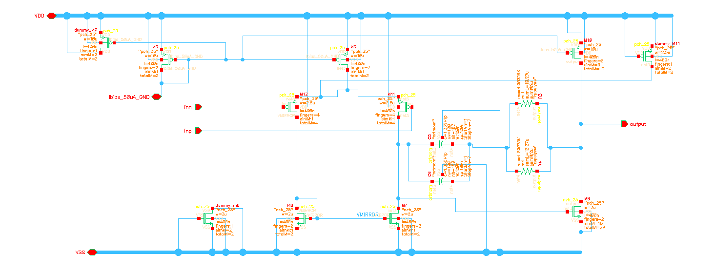
Envelop detector op-amp circuit
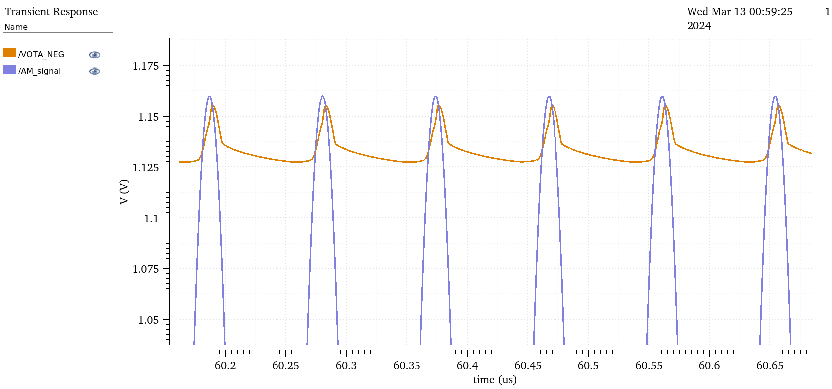
Detector output of four-tones 10.7MHz modulated signal
Sallen-Key Low-Pass Filter:
The output of the envelope detector is the desired audio signal. However, this signal contains significant high-frequency ripple caused by the charging process when the diode is on and the discharging process when the diode is off. If this ripple is directly applied to the power amplifier and speaker, it will introduce substantial noise.
To address this, an active Sallen-Key low-pass filter is used to eliminate the high-frequency noise. The frequency of the ripple is approximately equal to the carrier signal frequency of 10.7 MHz. The 3-dB cutoff frequency is set at 10 kHz, the cutoff frequency may drop down to 4.7 KHz for the maximum 30% variation on resistor and capacitor, but it still preserves most of the baseband audio signal while effectively attenuating the ripple. This ensures a clean audio output with minimal distortion or interference.
The amplifier uses a two-stage Miller compensation structure, with the unity-gain frequency set 1,000 times greater than the cutoff frequency, ensuring the accurate cutoff frequency.
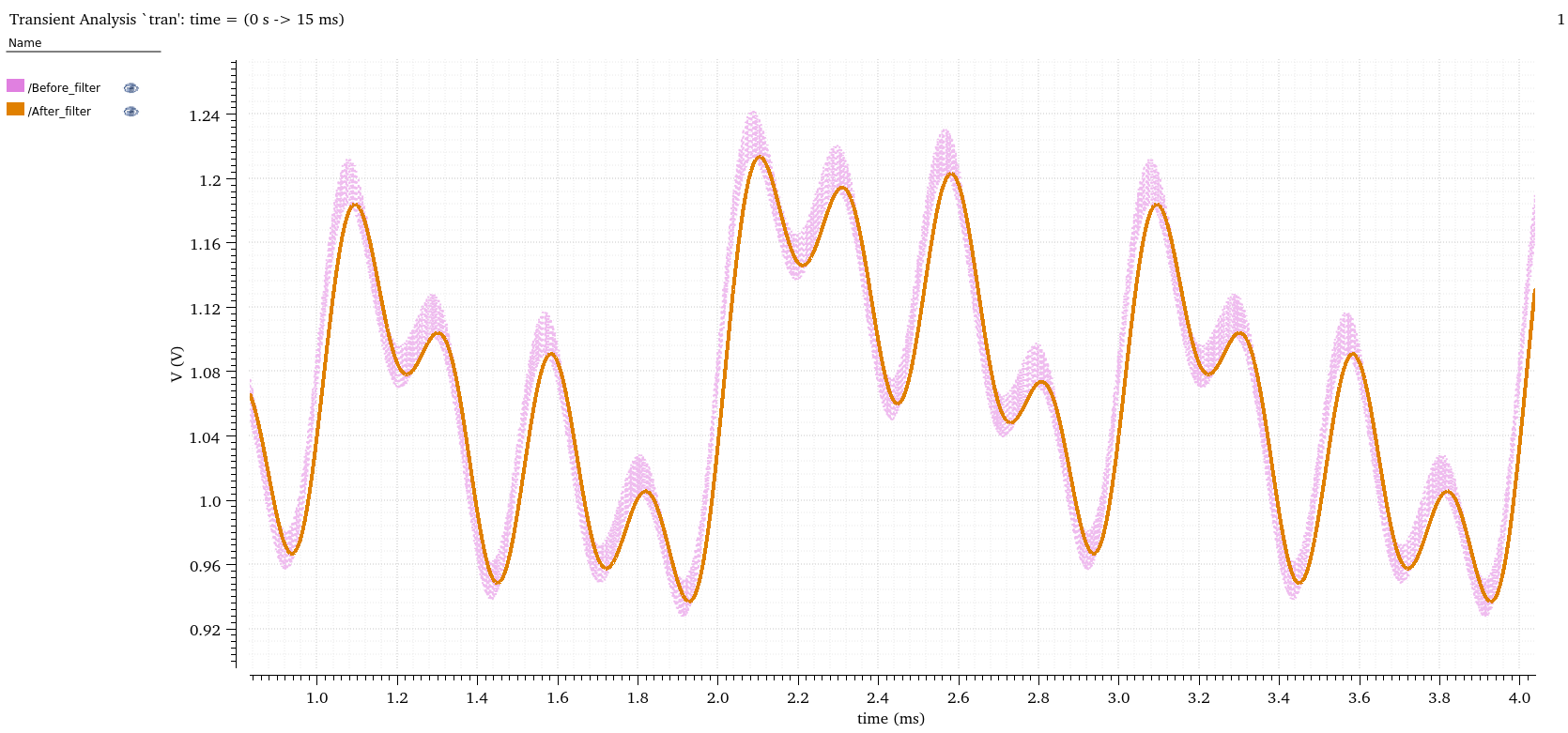
Left: ripple of detector output right:comparsion between detector output and filter output
Active low-pass filter OTA circuit
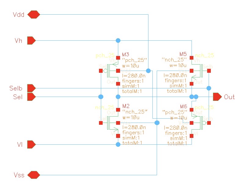
Transmission Gate Control and Cascode Current Mirror:
There are three transmission gates strategically placed in the circuit: one between the detector output and the RC network of the detector, another between the low-pass RC network and the filter input, and the third between the low-pass RC network and filter output.There are three transmission gates strategically placed in the circuit: one between the detector output and the RC network of the detector, another between the low-pass RC network and the filter input, and the third between the low-pass RC network and the filter output.
These transmission gates are controlled by the same enable signal generated by a Schmitt trigger from standard library, which effectively rejects noise from the off-chip source and stabilizes the control signal. When the transmission gates are enabled, the envelope detector and the low-pass filter's OTA utilize the on-chip RC network. Conversely, when the transmission gates are disabled, the on-chip RC network is disconnected, allowing the off-chip RC network to be used as a backup or for testing purposes.
A cascode current mirror is used to provide a precise reference current for both the envelope detector and the active low-pass filter.
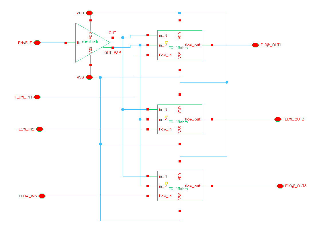
Left: three channel transmission gate block diagram right: cascode current mirror circuit