
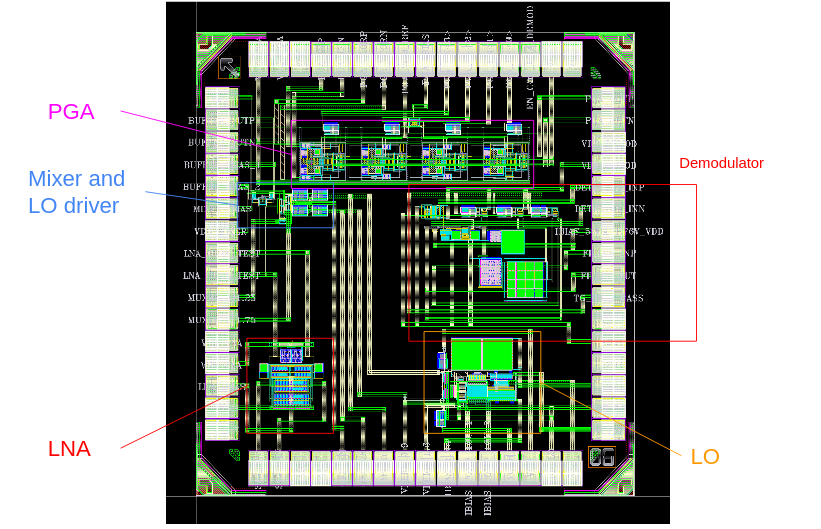
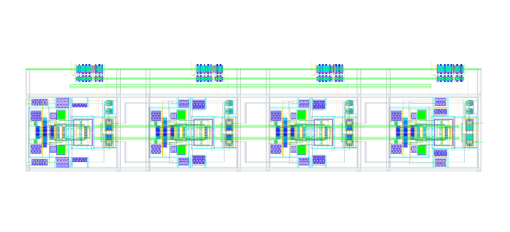
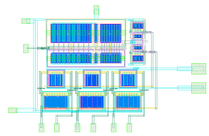
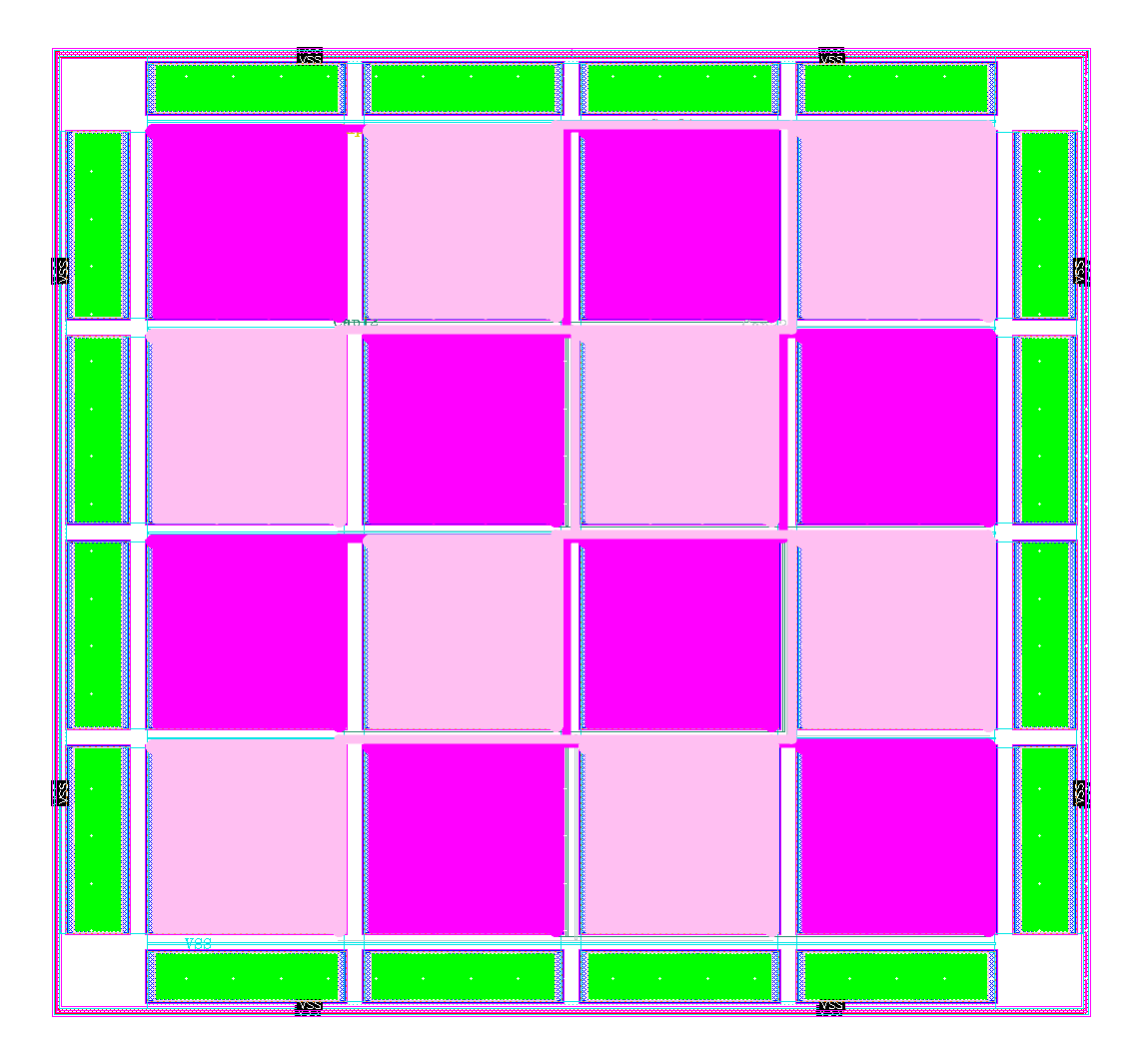
IC Layout
This page shows the details about the chip layout and each block layout.
Overall Chip Layout:
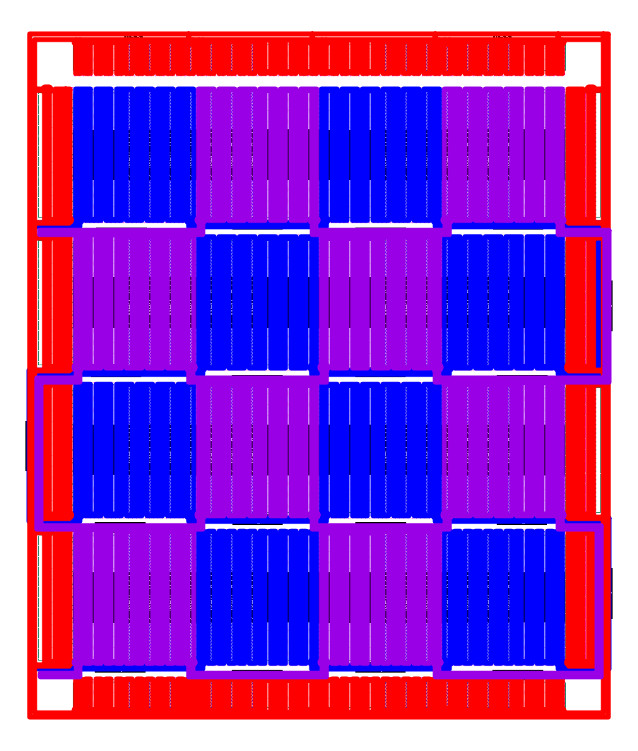
Low Noise Amplifier(LNA):
LNA layout is shown as below. This is a common-center layout, which mitigates mismatches and improves the robustness after fabrication
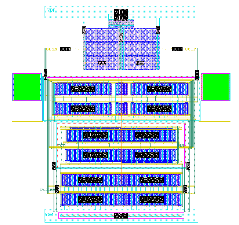
LNA Layout
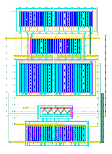
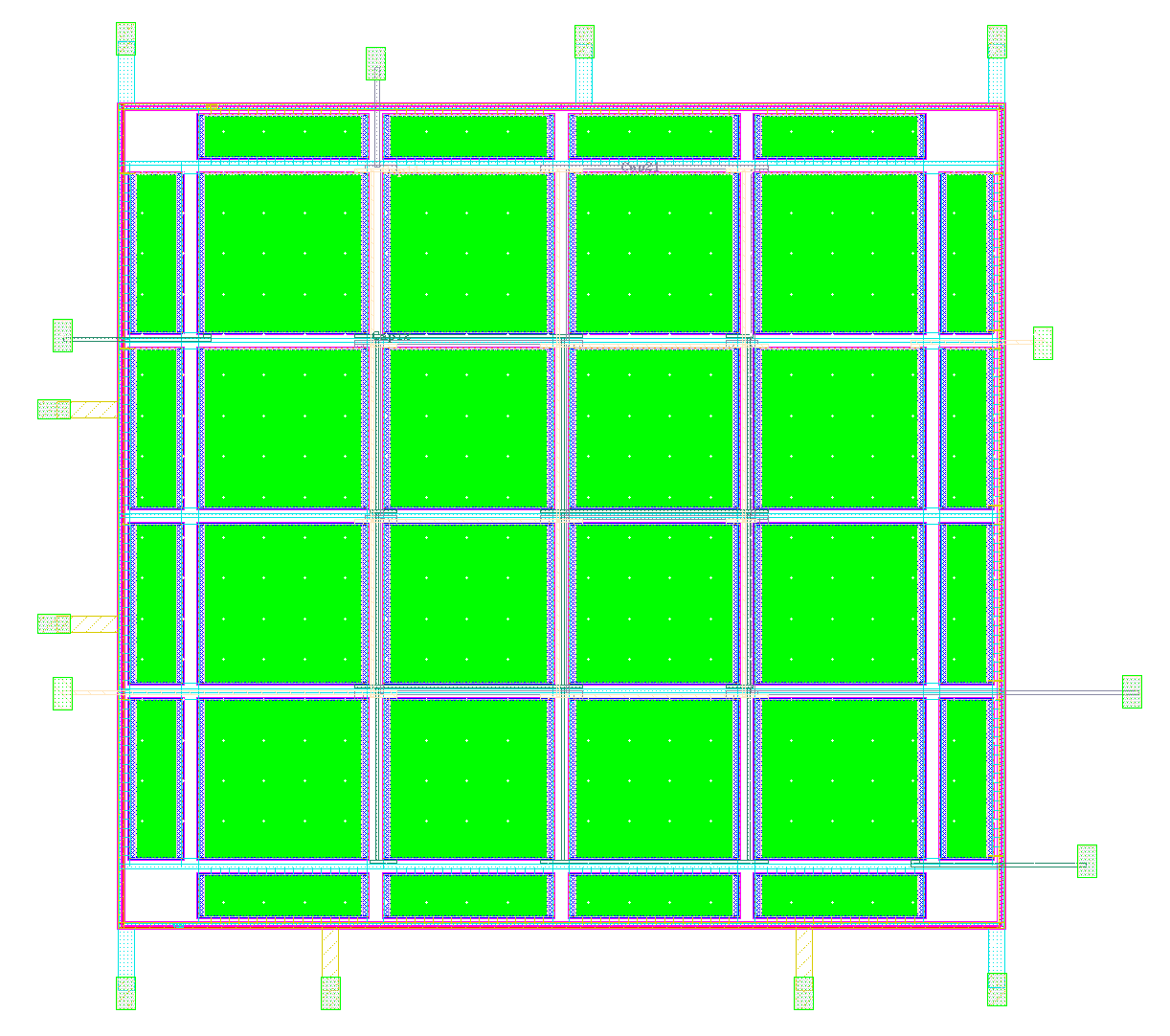
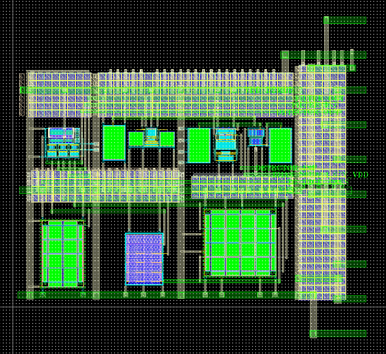
Mixer + Buffer:
Mixer + buffer layout is shown below.
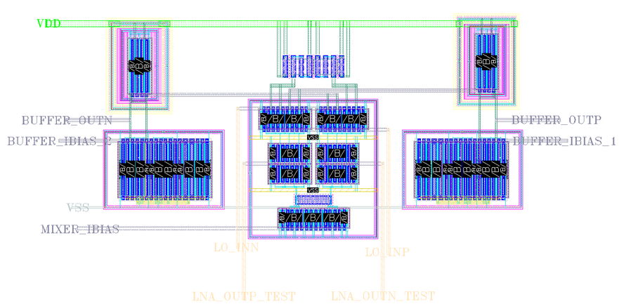
Mixer + Buffer Layout
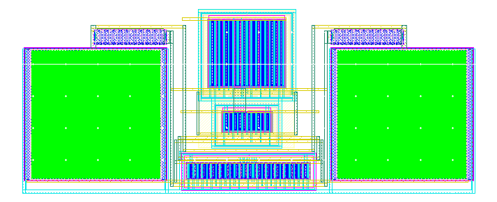
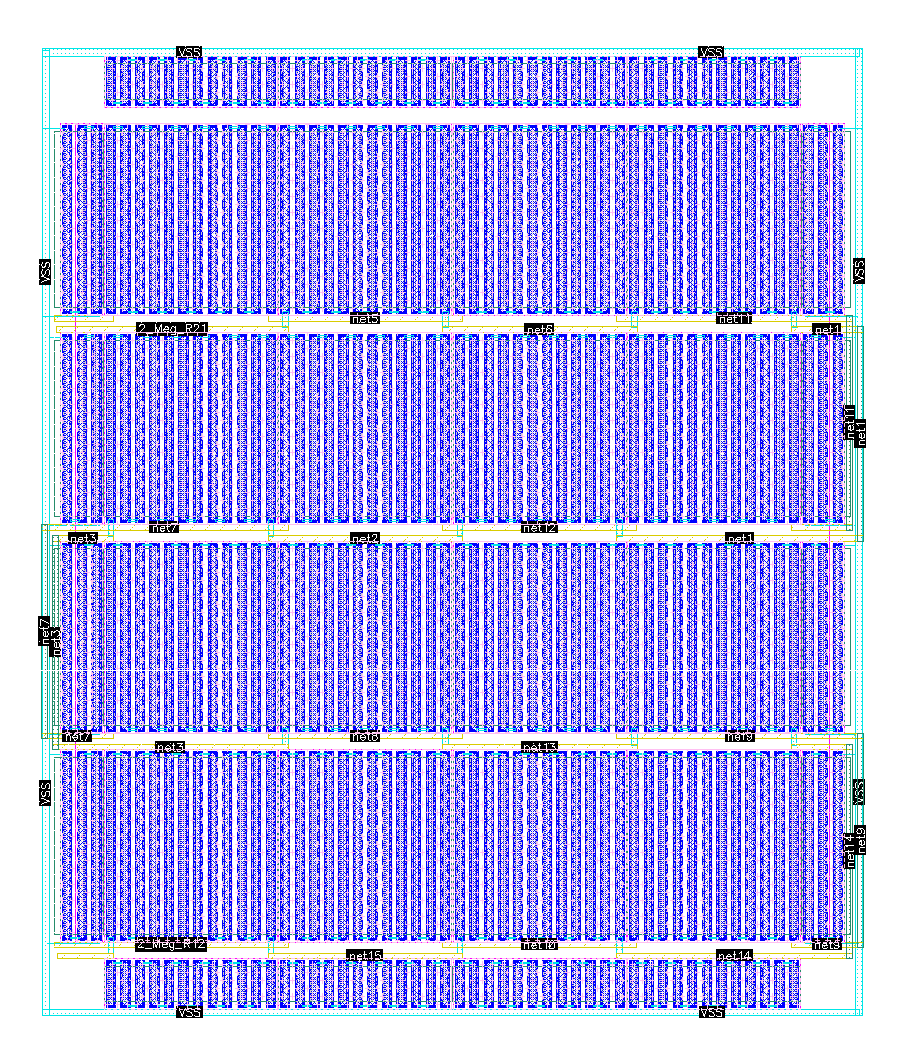
Voltage control oscillator(VCO):
VCO layout is as follows. Two current mirrors of the charge pump are mixed together as one slice to minimize current asymmetry, and comparator differential pairs are central symmetry to decrease offset.

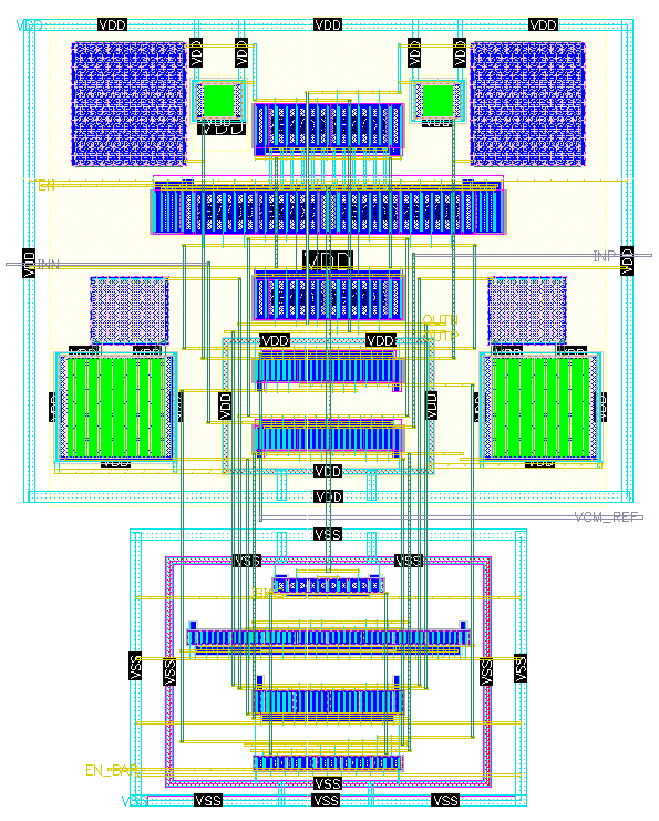
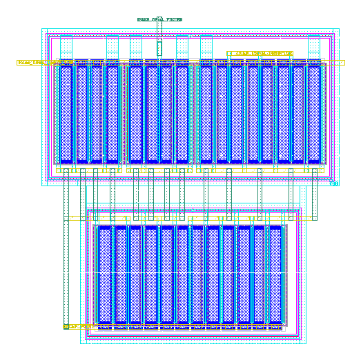
Programmable Gain Amplifier(PGA):
The PGA layout is shown as below
Single-Stage Core OTA Layout
Four-Stage PGA Layout
Demodulator:
Envelop detector layout
Active low-pass filter OTA layout
Current mirror layout
Schmitt-trigger controlled transmission gate layout
Common Centroid Layout for resistor in sallen-key low-pass network, surrounding part is dummy, inside same color parts are connected
Common Centroid Layout for capacitor in sallen-key low-pass network, surrounding part is dummy, inside same color parts are connected
The entire layout of demodulator