
PCB Design
This page shows the details about the PCB design.
The PCB is designed using KiCad and is designed to achieve the following things:
- 1) Including off-chip blocks which are antenna, crystal filter, power amplifier, and speaker.
- 2) Providing separated power domains as well as biasing and reference voltages .
- 3) Leaving enough ground pins for the probe, enough testing pins of each block with output unit gain buffer, and enable pins to bypass blocks or do PGA gain control.
- 4) Doing enough backup plans such as leaving a transformer to do differential to a single output, offset compensation for PGA, PLL interface for VCO, and low pass filter for the demodulator.
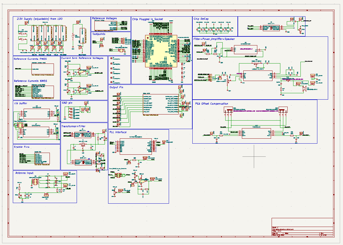
PCB Schematic
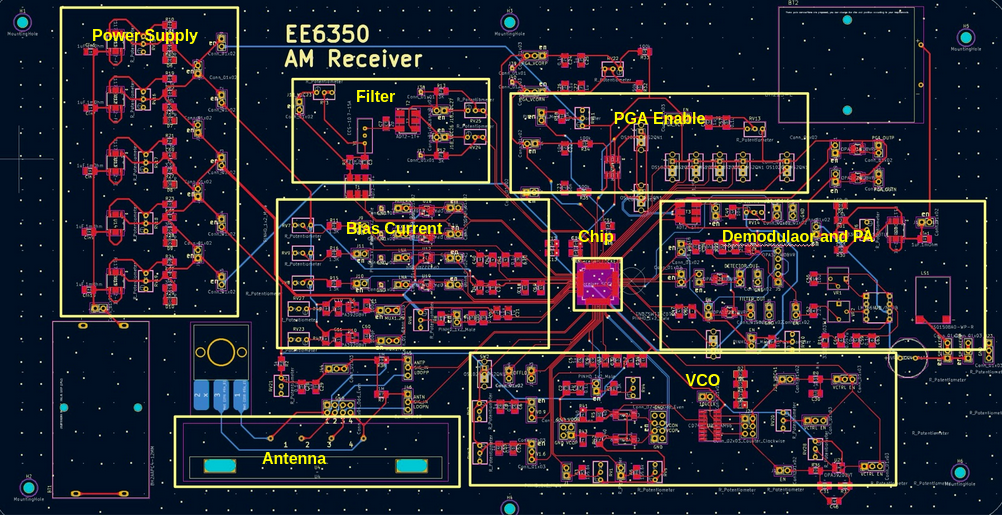
PCB Layout
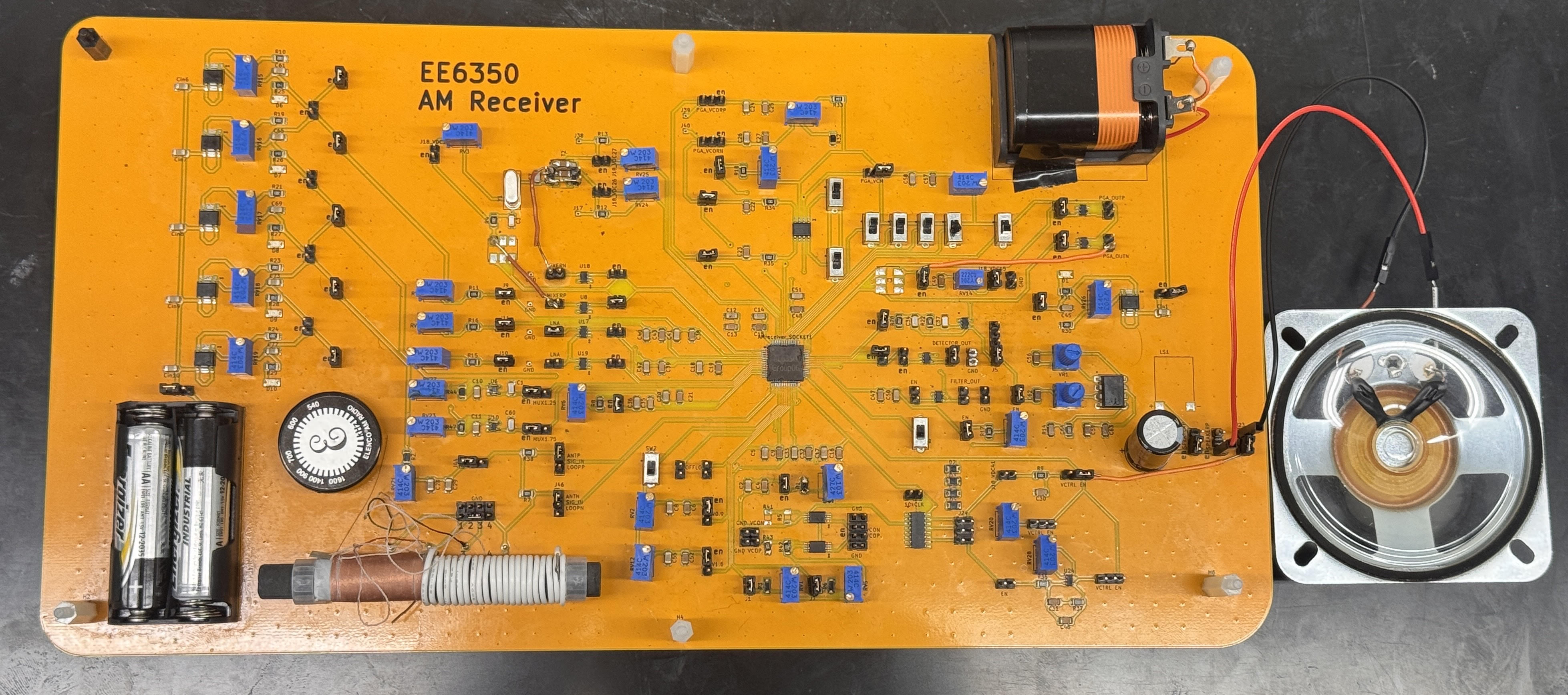
Whole system on PCB