
PCB Design
KICAD was used to design a two-layer PCB to test the chip's functionality and connect it with other peripheral circuits.The dimension of the PCB is around 20cm × 15cm.
Figure 1 shows the schematic for the whole PCB.
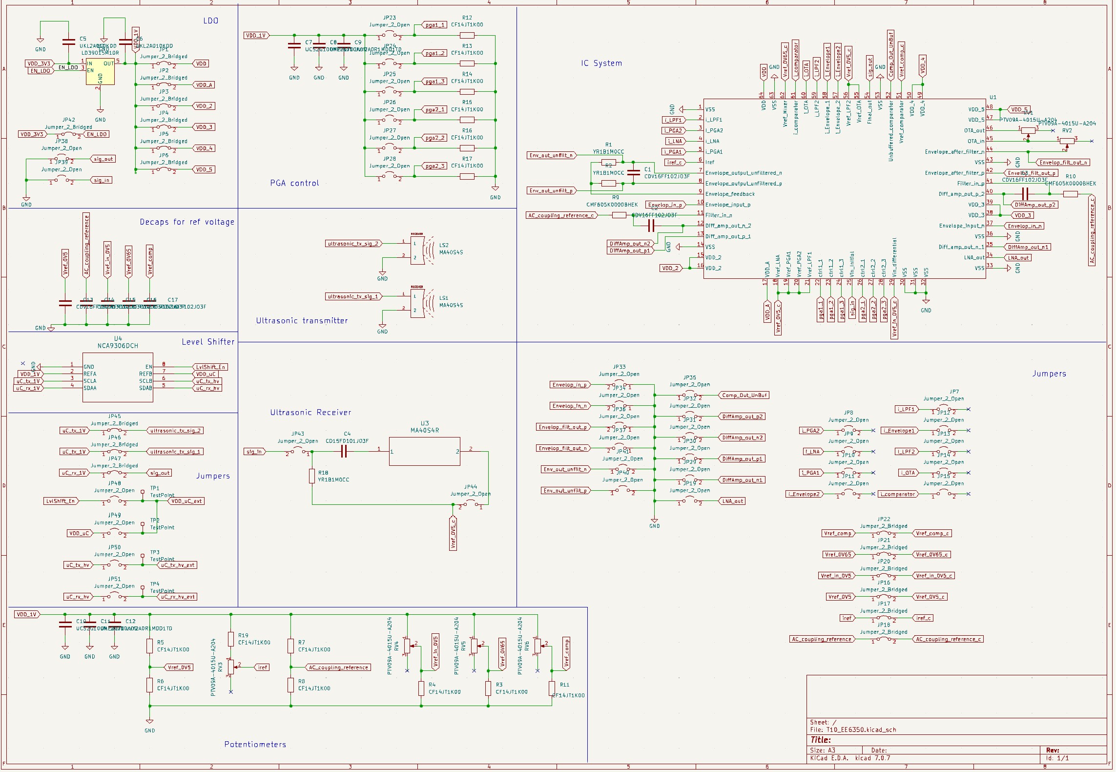
Figure 1: PCB Schematic
LDO: The PCB has an LDO to regulate a 3.3V input supply to a 1V output supply for the receiver.
PGA Control: There are 6 jumpers on the PCB for the 6 PGA control signals (2 sets of 3 bit control).
IC System: This section has the socket for the ultrasonic receiver device, and some peripheral components. This includes resistors and capacitors for the AC coupling of the signal from the output of the amplifier stages to the input of the first LPF stage. This also includes potentiometers to form an adjustable resistive feedback network of the OTA at the output of the envelope detector.
Decaps for the ref voltage: For the voltage references generated on the board. Jumpers: To add flexibility while testing.
Ultrasonic transmitter/receiver: On board ultrasonic transmitter is present to enable round trip range measurement (signal sourced from a mirco-controller) if needed. Ultrasonic receiver to receive the 40kHz signal and feed to the device.
Potentiometers: To adjust the reference voltages to the blocks in the device. This section also has the decaps for the voltage supply.
Jumpers: Top act as test-points and for added flexibility/wiring for post-silicon debugging.
Figure 2 shows the block diagram of PCB Layout.
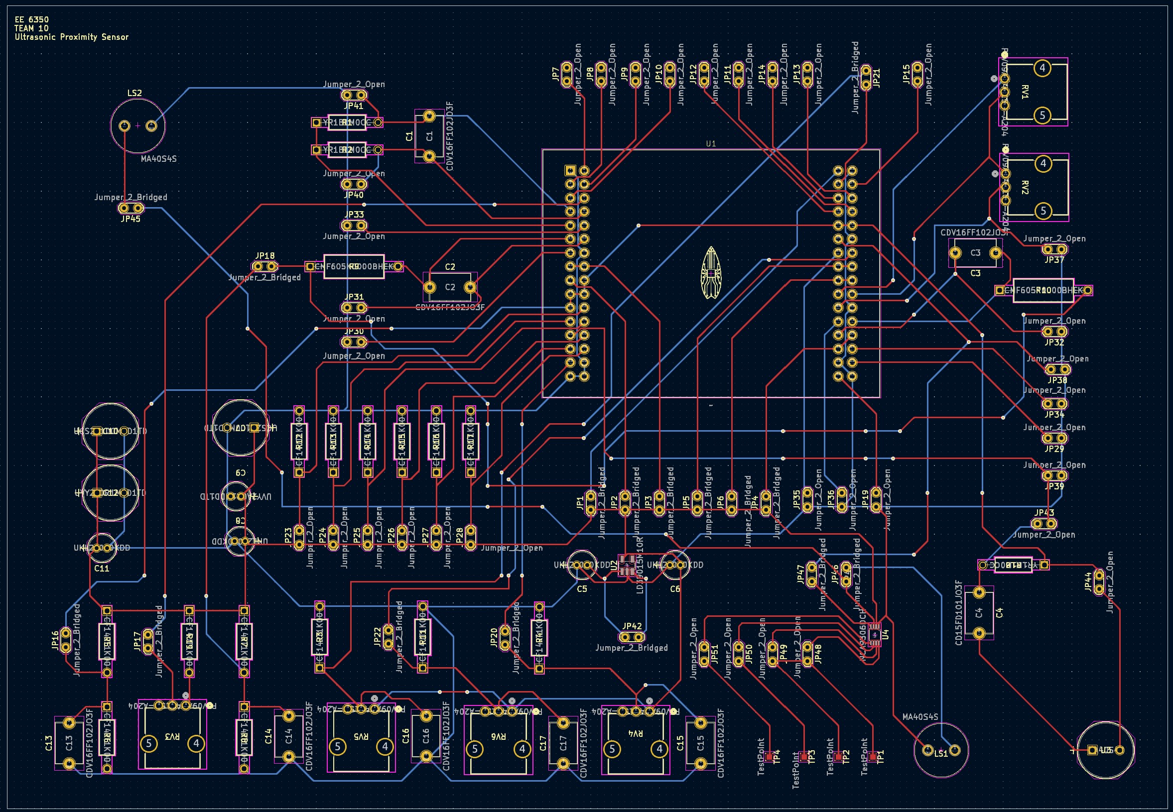
Figure 2: PCB Layout
Figure 3 shows the 3D view of PCB Layout.
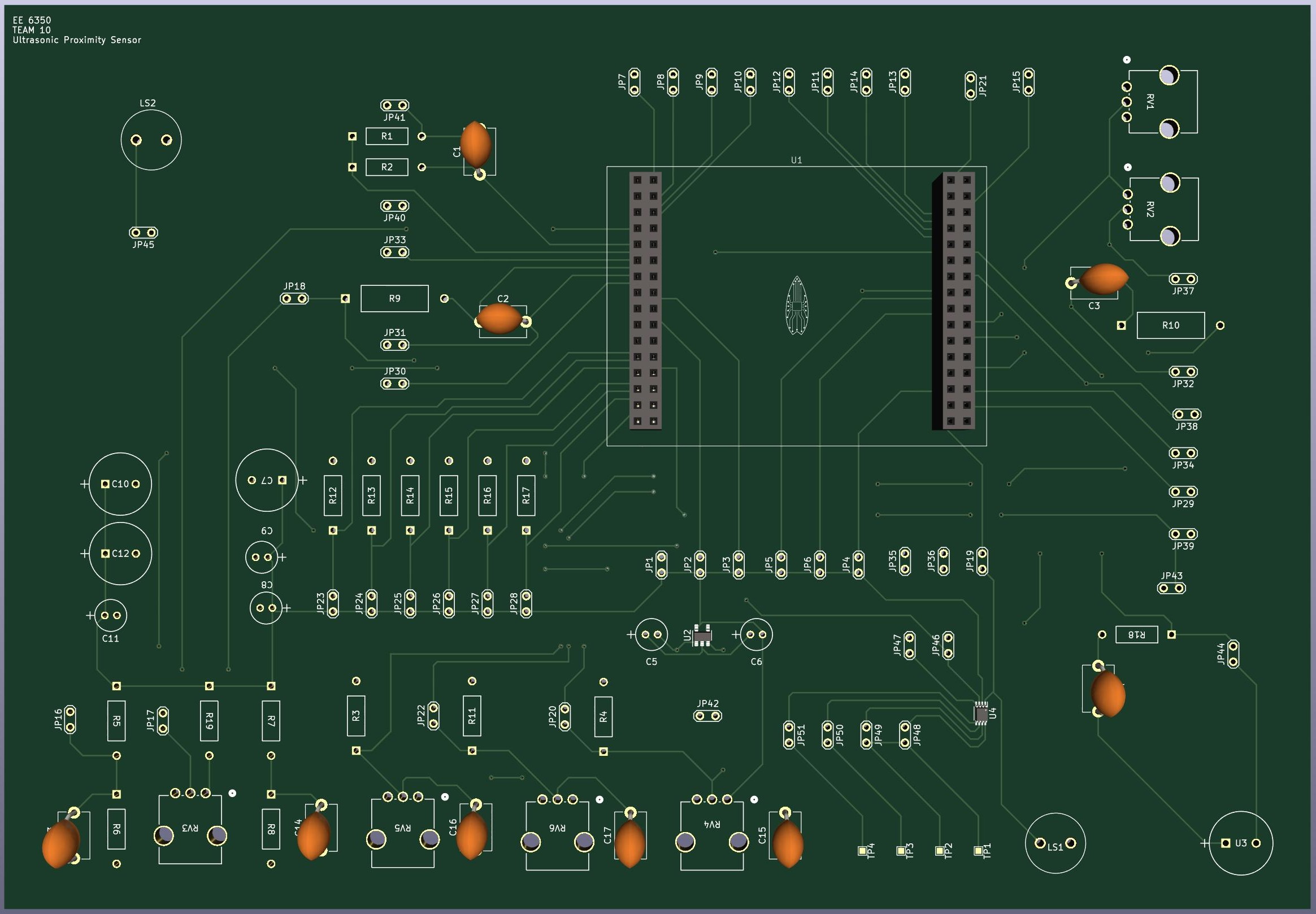
Figure 3: 3D View of PCB
Figure 4 shows the complete PCB, populated with all components.
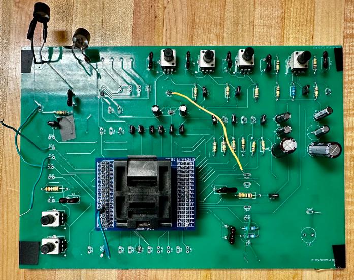
Figure 4: PCB Assembly