
IC Design and simulation
Low Noise Amplifier(LNA)
Low noise Input with a gain of 14dB, using a 2 stage opamp configuration with the first stage of differential pair and second stage of a common source. Input referred noise of 8 uV across the bandwidth of the system.
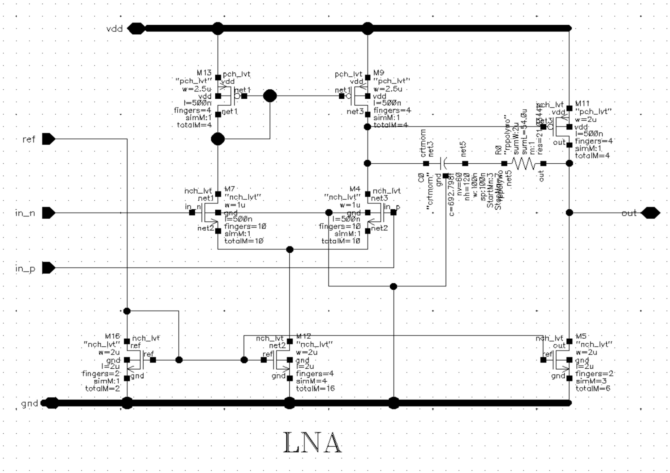
Figure 1: LNA Schematic
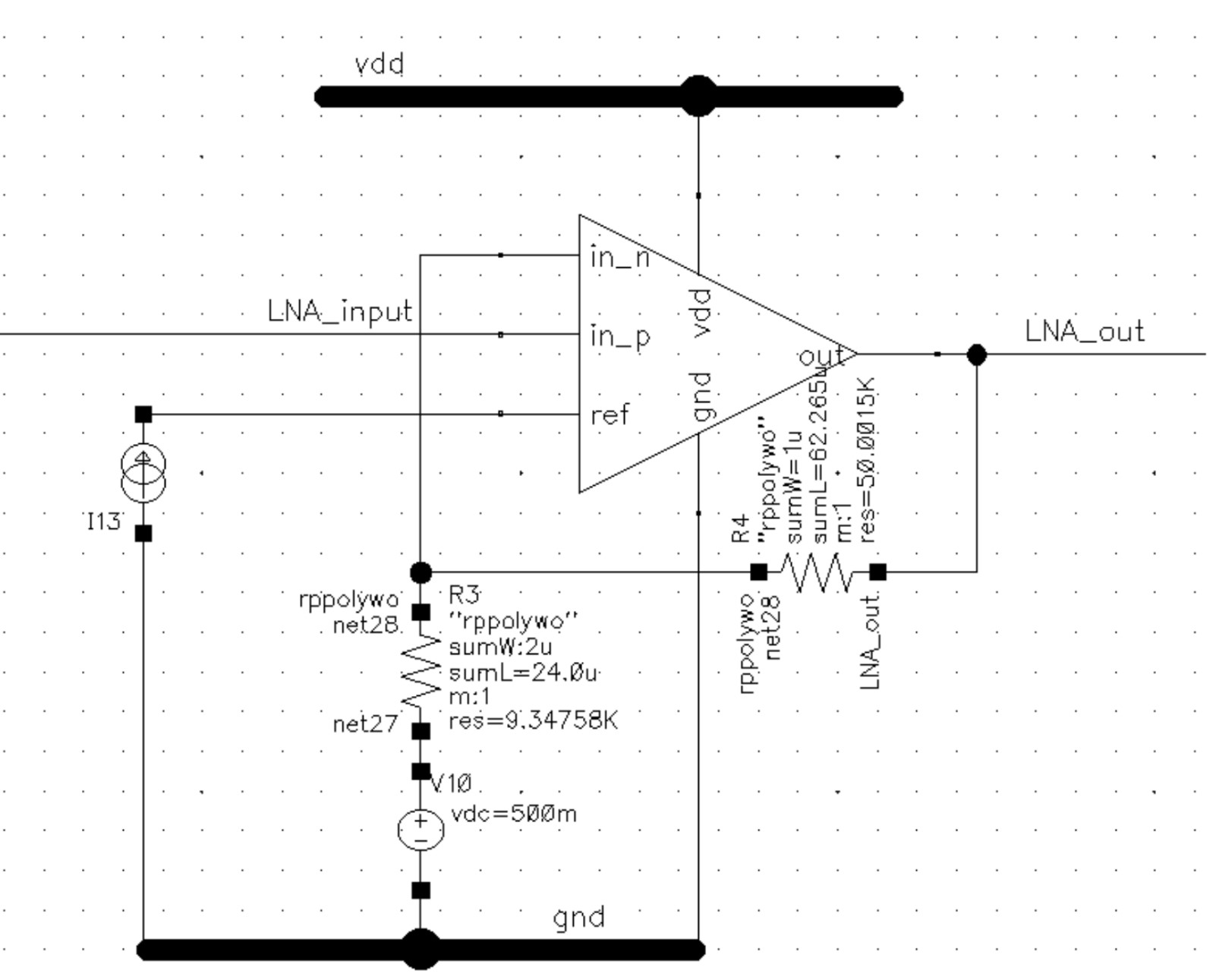
Figure 2: LNA close loop with negative feedback
Multi-corner simulation LNA loop gain varied from 30.53dB (Best corner) to 21.66 dB (worst corner), phase margin varied from 84.35 (worst corner) to 100 (Best corner) degrees. Bandwidth varied from 7.79MHz (Best corner) to 3.97 MHz (Worst corner).
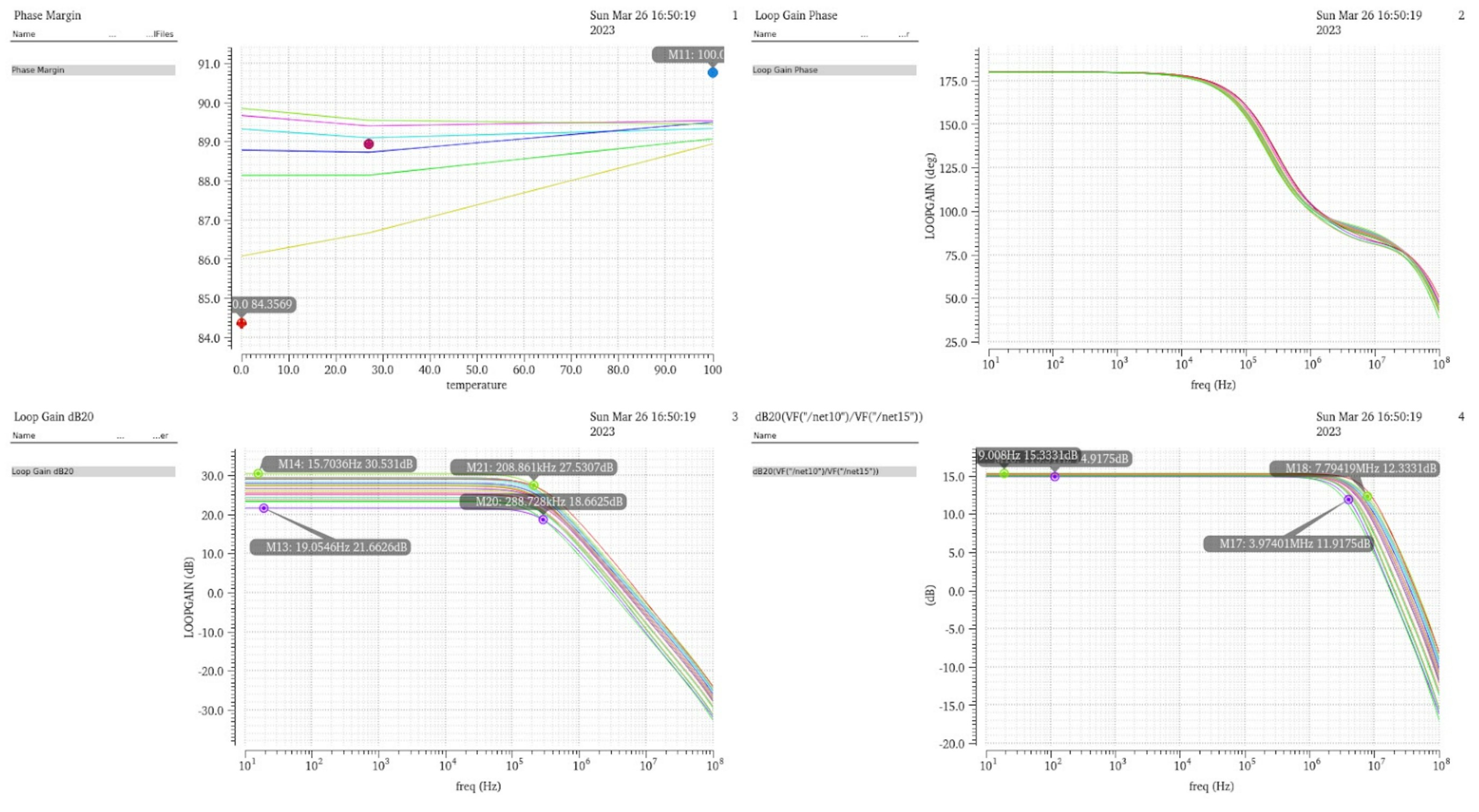
Figure 3: LNA Simulation
Programmable-gain amplifier(PGA)
PGA is the combination of the Differential Amplifier and transmission gate to the resistive network for gain control. The control logic is to add parallel feedback resistance thus decreasing the input resistance and increasing the gain. The PGA gain range is from 0 to 20 dB, and two stages of PGA provide a maximum of 40dB gain and a total 6 levels of gain variation (0 dB, 6dB, 10dB, 20dB, 30dB, and 40dB)
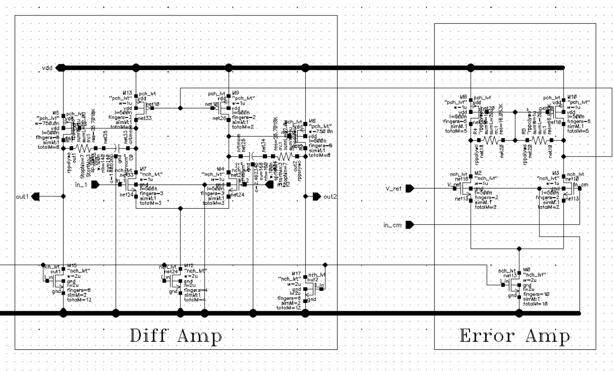
Figure 4: PGA Differential Amplifier
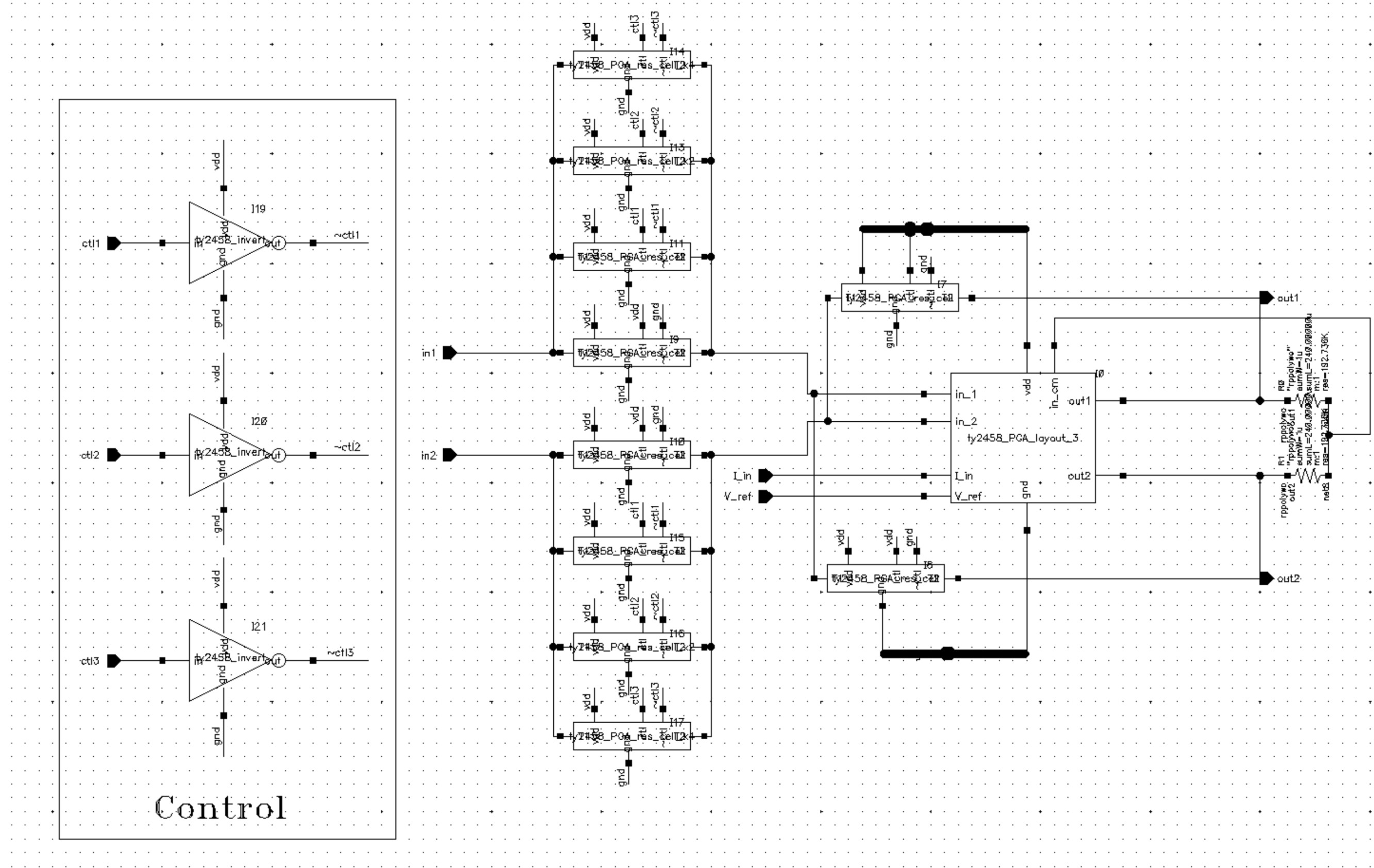
Figure 5: Complete PGA structure
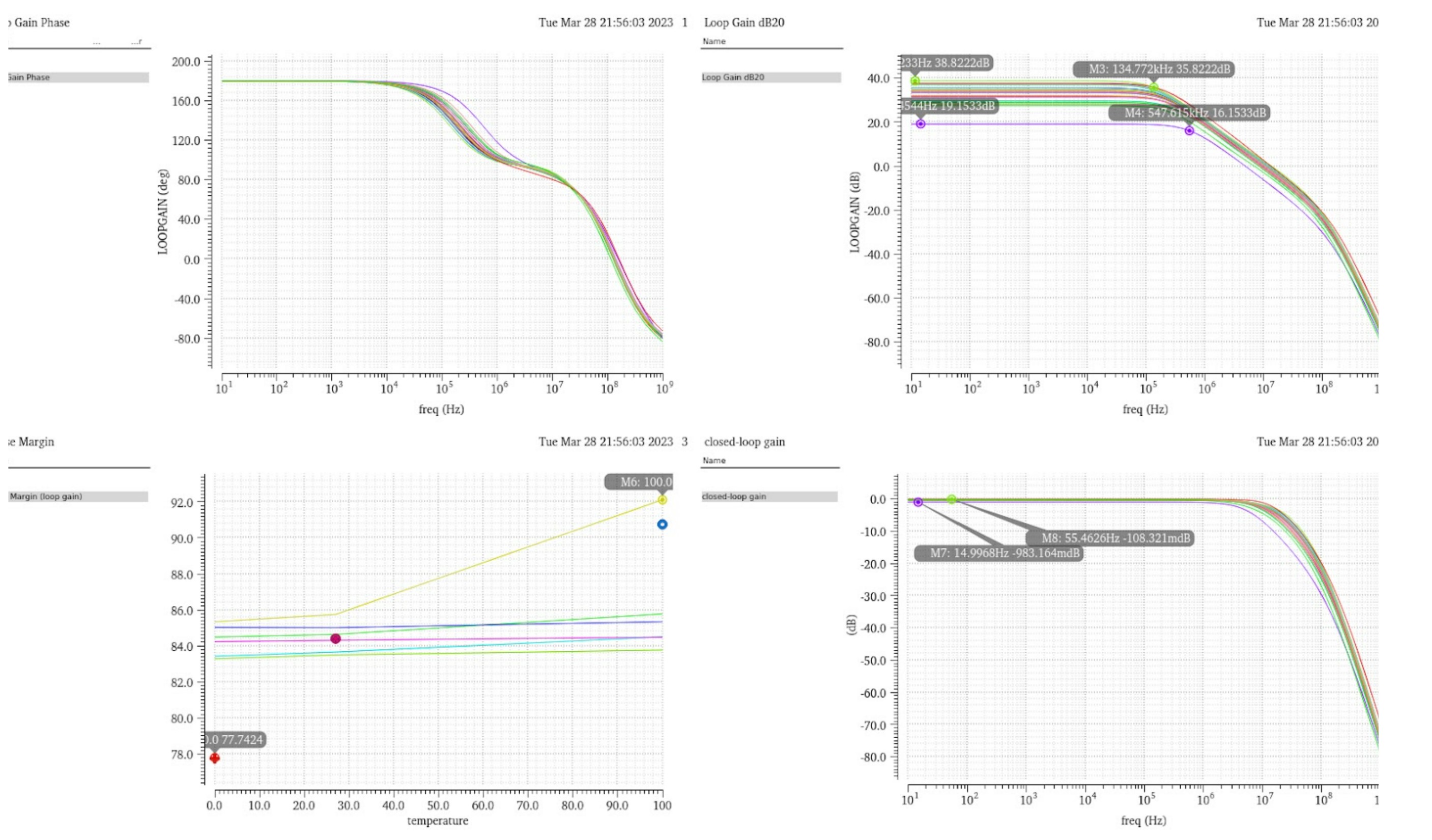
Figure 6: PGA Simulation
Multi-corner simulation single-stage PGA gain is varied from 19.15 dB to 38.82 dB, bandwidth varied from 5.9 MHz to 16.9 MHz, and Input referred noise varied from 52uV to 70uV.
Low Pass Filter(LPF)
The LPFs are 2nd order Chebyshev filters, realized using a fully differential Tow-Thomas Biquad.
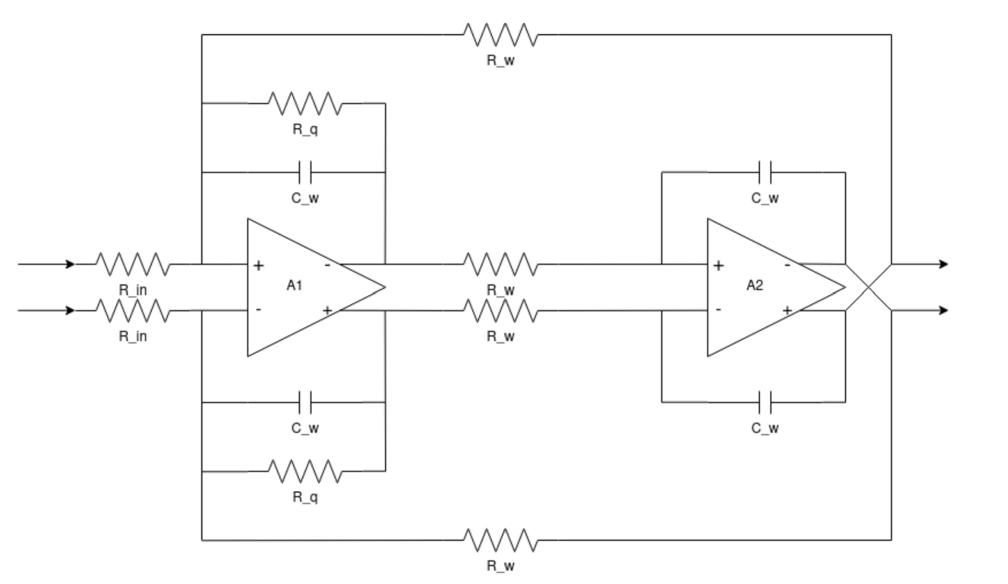
Figure 7: Filter Structure
The amplifier A1 functions as a lossy integrator (with RC feedback) and A2 acts as a regular integrator (with resistive feedback). The outer feedback closes the loop and sets the natural frequency of the filter (1/R_w*C_w). R_q in the lossy integrator sets the Q of the filter and R_in sets the filter gain.
A2 and A2 are fully differential OTAs realized using a Differential amplifier with common mode feedback (common mode detection + error amp).
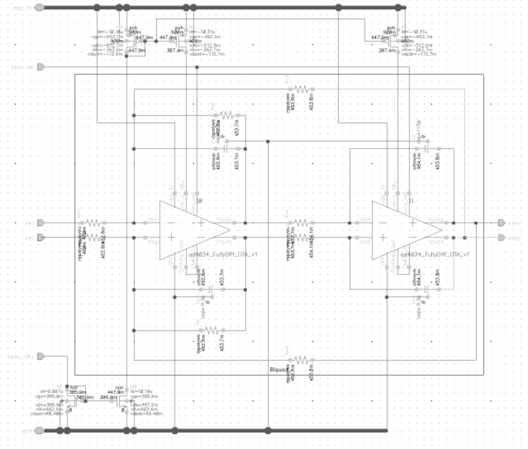
Figure 8: Fully Differential OTA (A1/A2)
The fully differential amplifier is a 2 stage differential Miller OTA. The common mode detection is done simply using large resistors connecting the differential outputs.
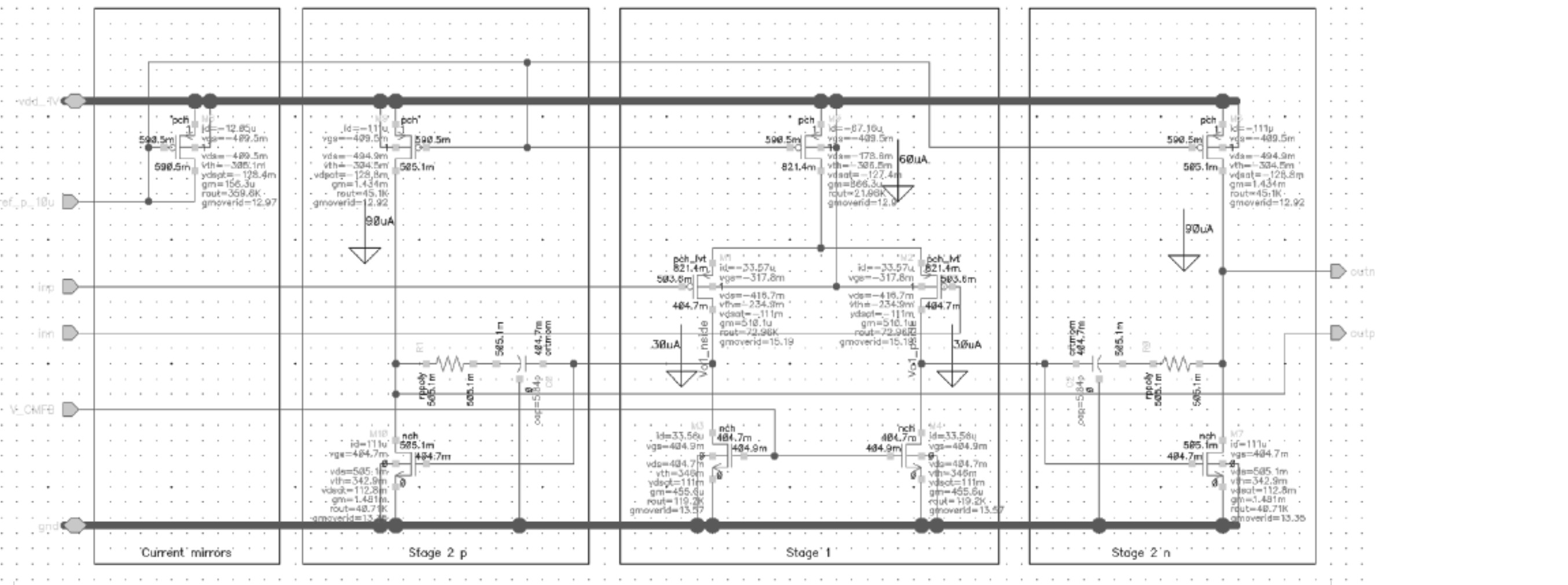
Figure 9: Differential Amplifier core (A1/A2)
The error amplifier for the common mode feedback is a differential pair with a diode connected load (for maximum error amp bandwidth, preserving the phase margin in the common mode path). LPF1 has a cutoff frequency of 110kHz.
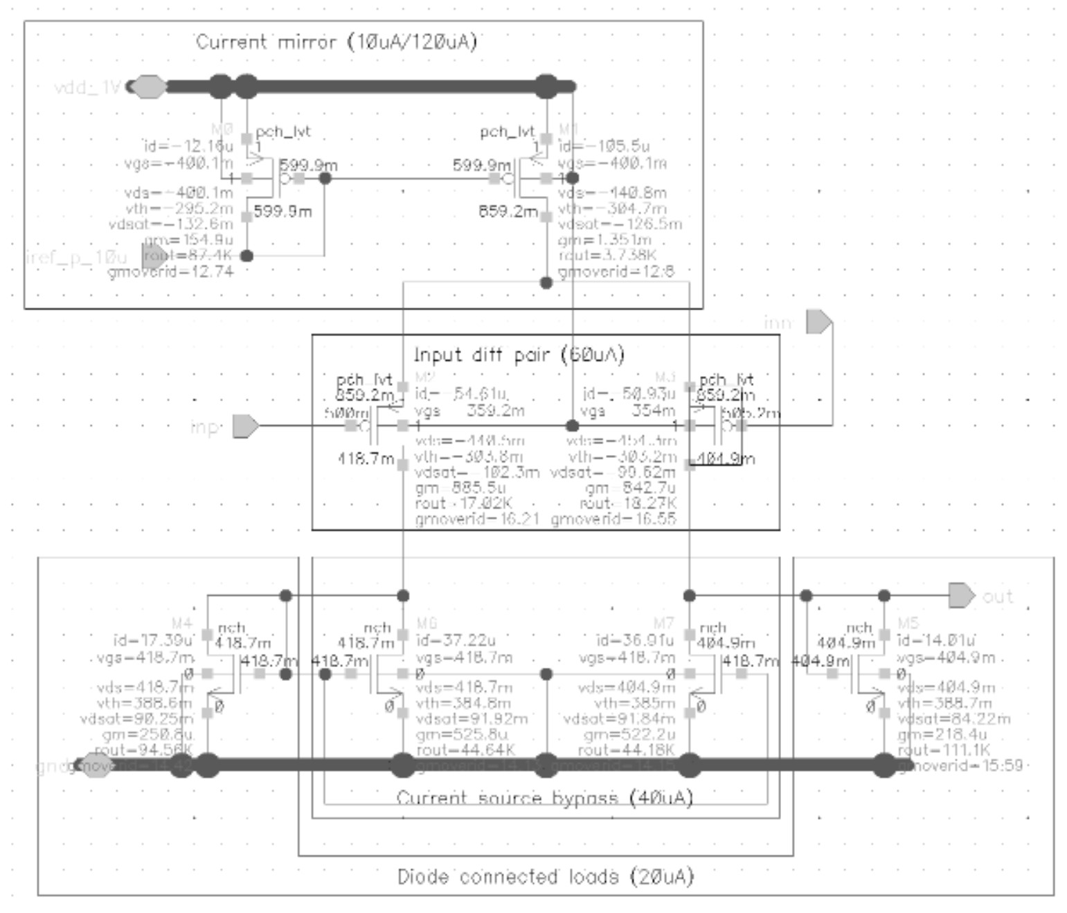
Figure 10: Error amp, Common mode feedback for A1/A2
LPF1 is used to filter out high frequency noise, while passing the desired 40kHz signal. It has a typical cutoff frequency of 110kHz (48kHz to 190kHz across PVT). The LPF cutoff variation comes largely from the PVT variation of the passive resistors and capacitors in the block.
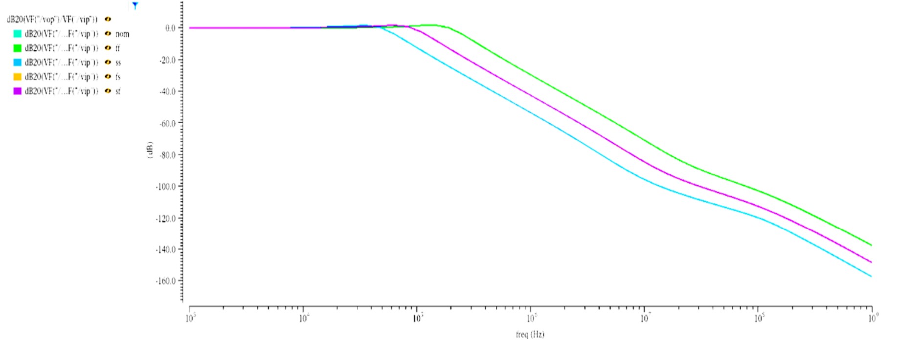
Figure 11: LPF1 Simulation
LPF2 is used to filter out the spurious 80kHz ripple from the envelope detector, while preserving the low frequency envelope (10Hz to 100Hz). It has a typical cutoff frequency of 10kHz (6kHz to 17kHz across PVT).
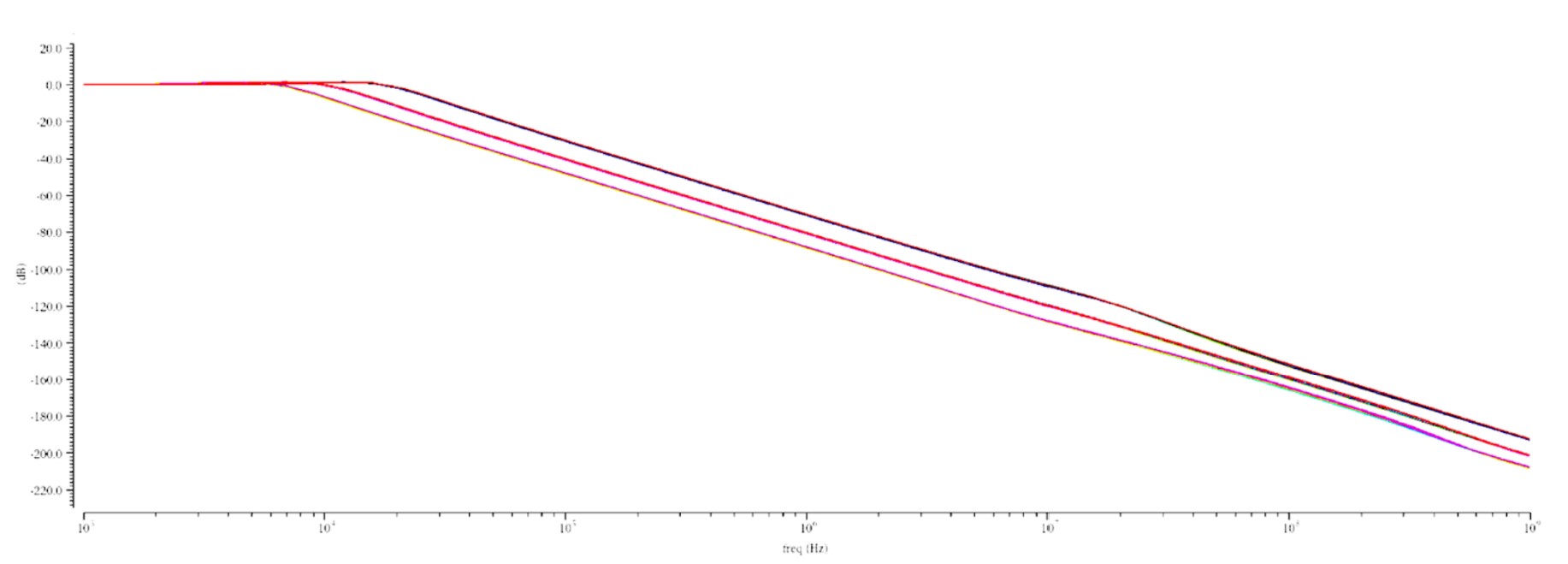
Figure 12: LPF2 Simulation
Envelope Detector
The Envelop Detector uses using Gilbert cell mixer to self-mix the input signal to create the envelope of the input signal with the low-frequency characteristic. The full envelope block includes a Gilbert cell mixer for the self-mix, a low pass filter cutoff frequency at 10KHz to filter out the 80K Hz signal generated from the self-mix 40K Hz frequency and keeps the desired low frequency (lower than 1K Hz) envelop, and an additional OTA for different corner gain variations observed in the simulation.
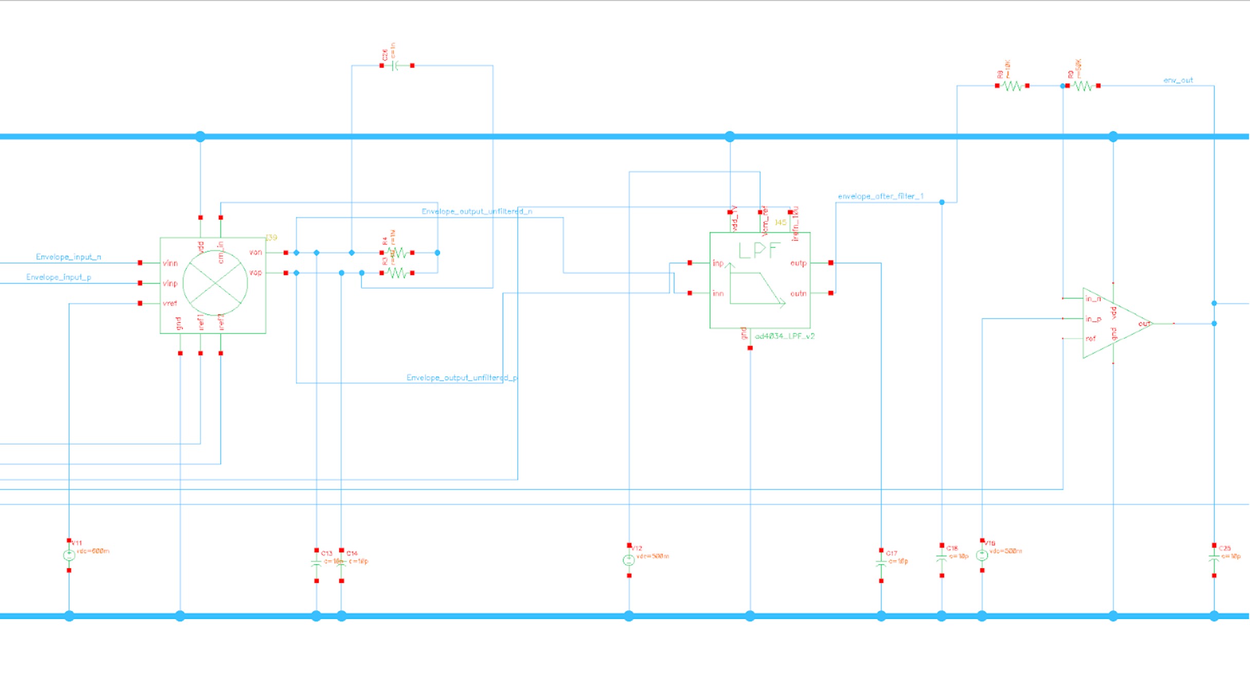
Figure 13: Envelope Detector Schematic
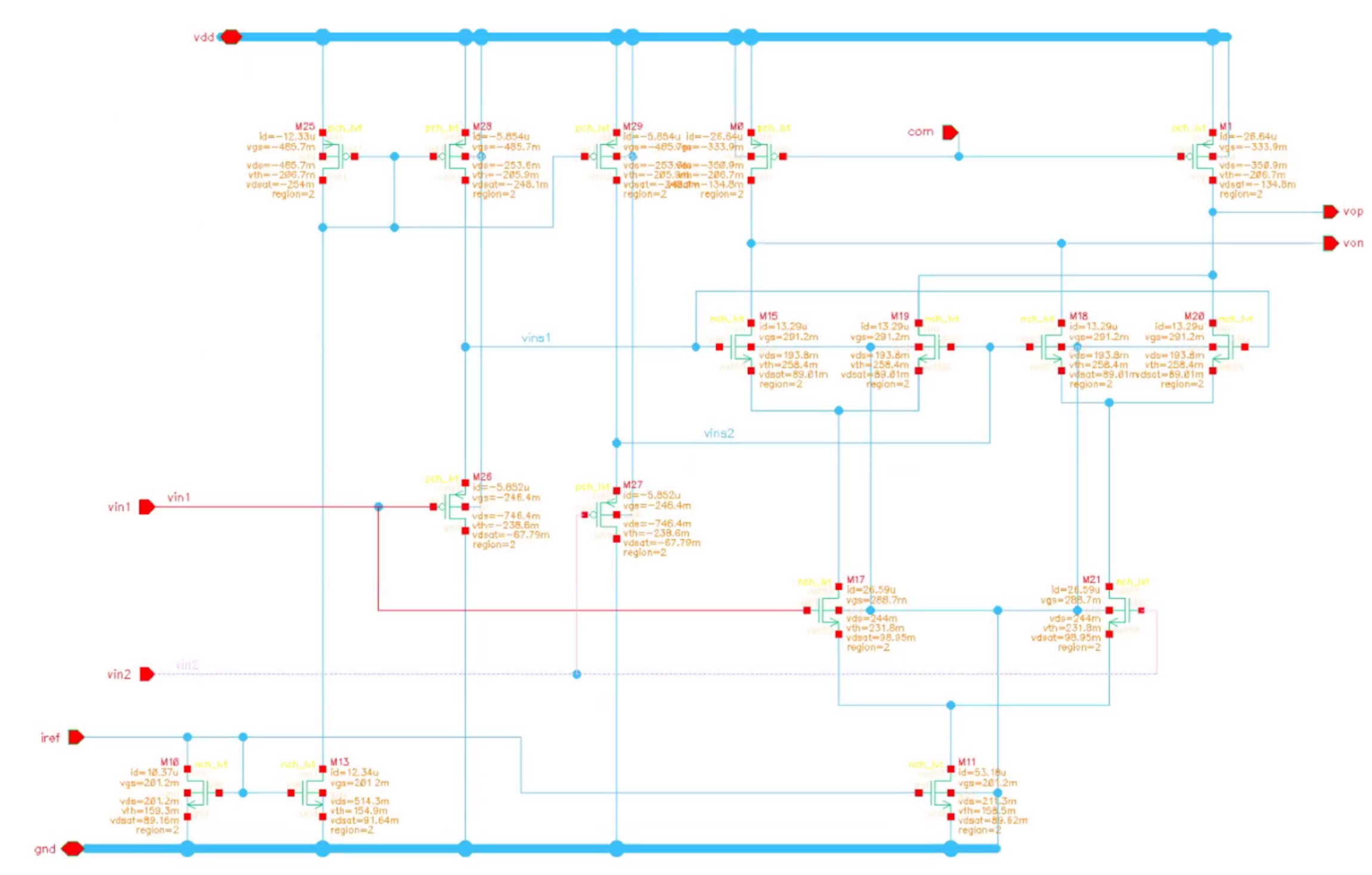
Figure 14: Gilbert cell Mixer Schematic
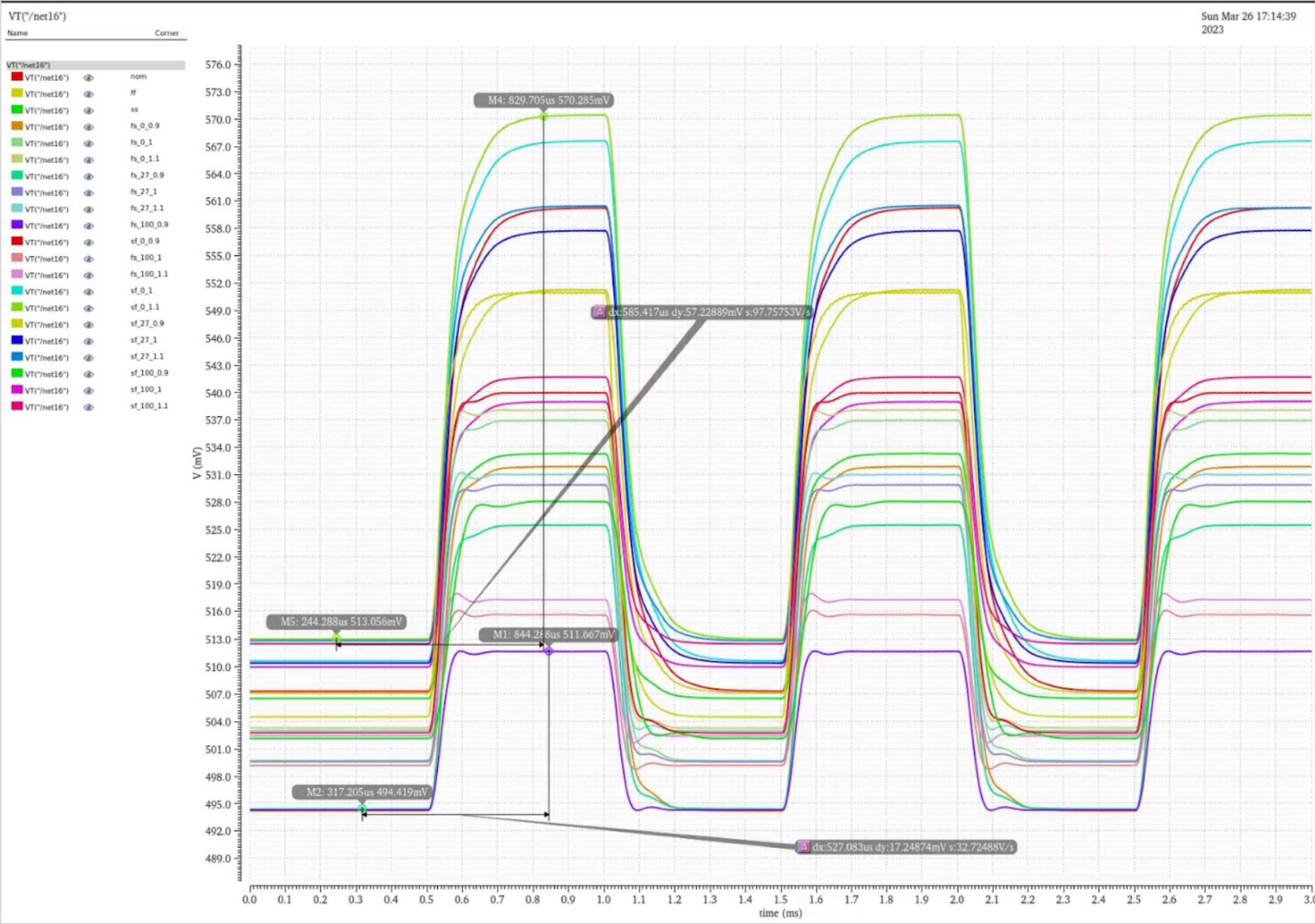
Figure 15: Envelope Detector Simulation
With Input of the 30mV amplitude sine wave, the output envelope amplitude is varied from 20mV (fs corner) to 57mV (sf corner) due to the different process corner changes the output impedance affects the gain from the envelope detector.
Comparator
The comparator uses a hysteresis comparator structure with a hysteresis of +/- 15mV to provide a more stable comparison that can exclude the noise from the input signal. A buffer will also be added to the output of the comparator to buff the signal for accurate logic output.
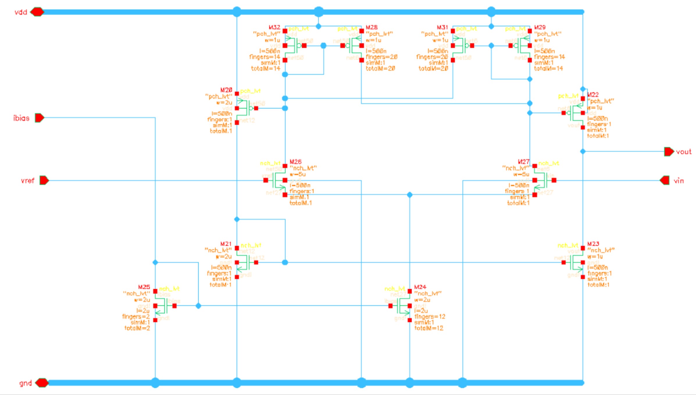
Figure 16: Hysteresis Comparator Schematic
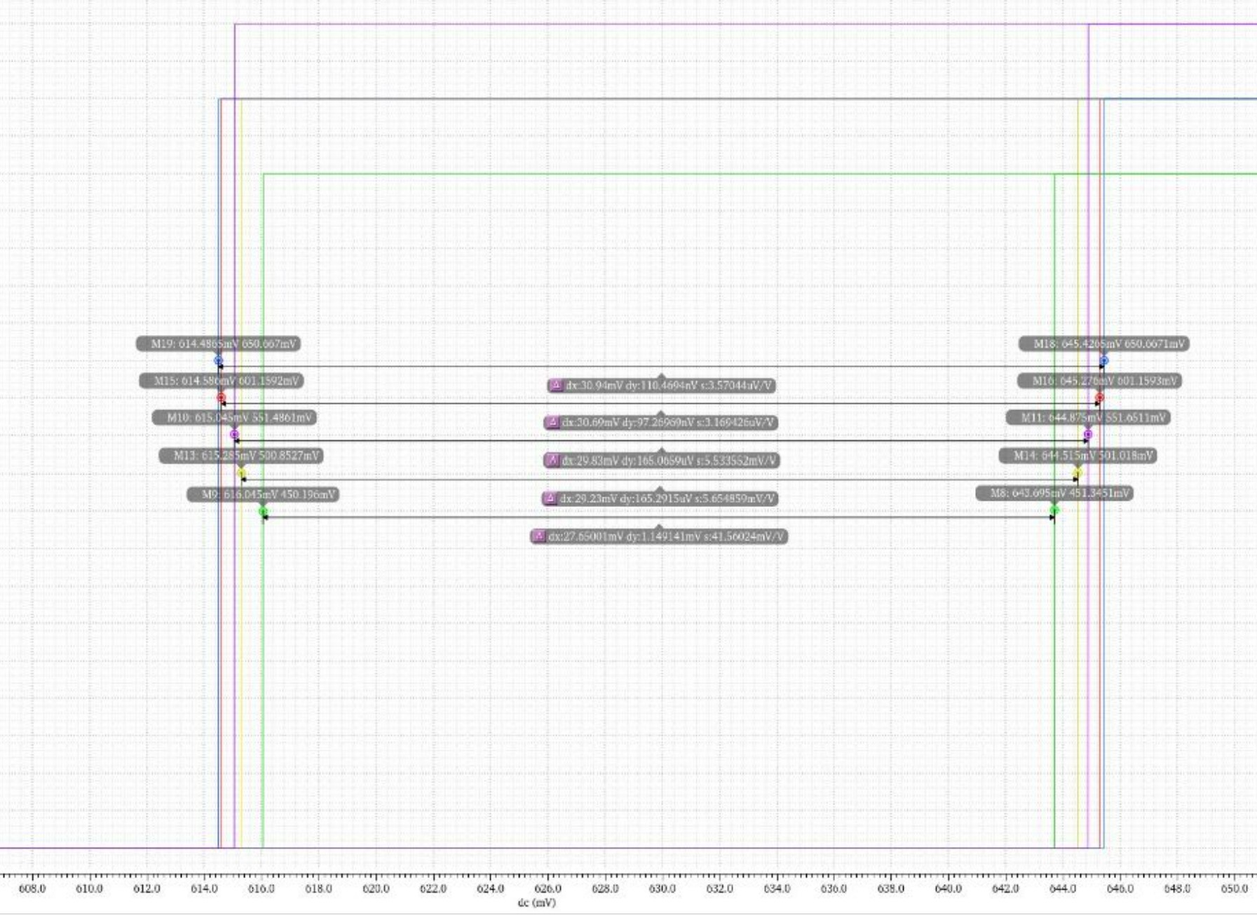
Figure 17: Hysteresis Comparator Simulation
Comparator simulation across the different corners sees a very small variation, with the hysteresis varied from +/- 13.8 mV to +/- 15.45 mV.