
IC Layout
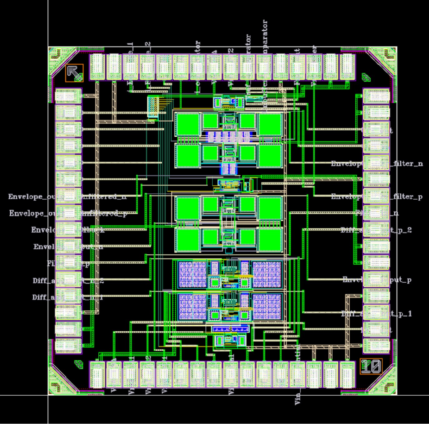
Figure 1: Top-level layout without decoupling and metal fill
The system layout is tried to be consistent with the 2D symmetric principle, with the signal chain in the middle and decoupling capacitors filling the empty left and right parts of the layout. High gain stages (LNA, PGA, and OTA) output is 90 degrees with its input to avoid the coupling.
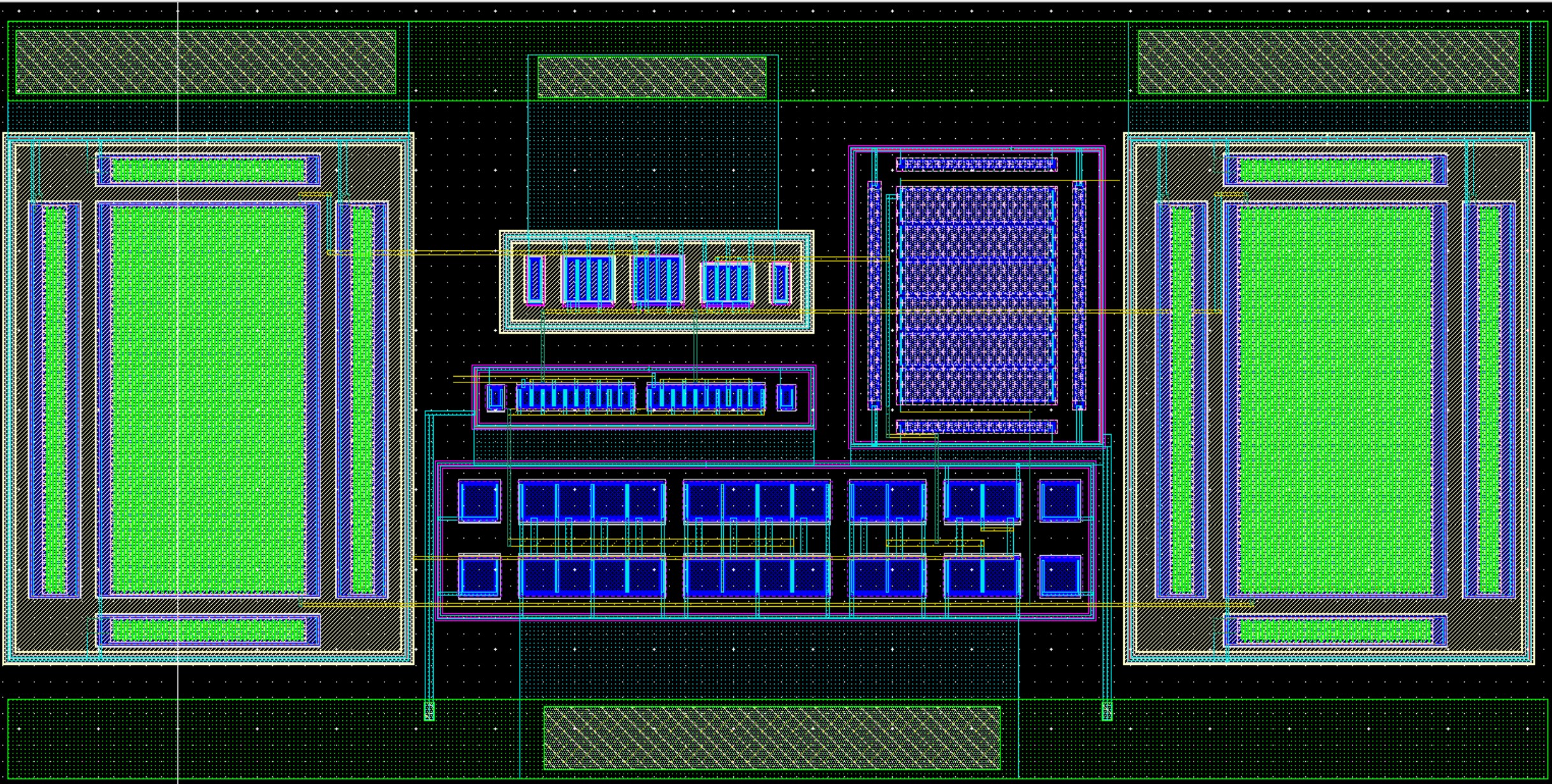
Figure 2: LNA Layout
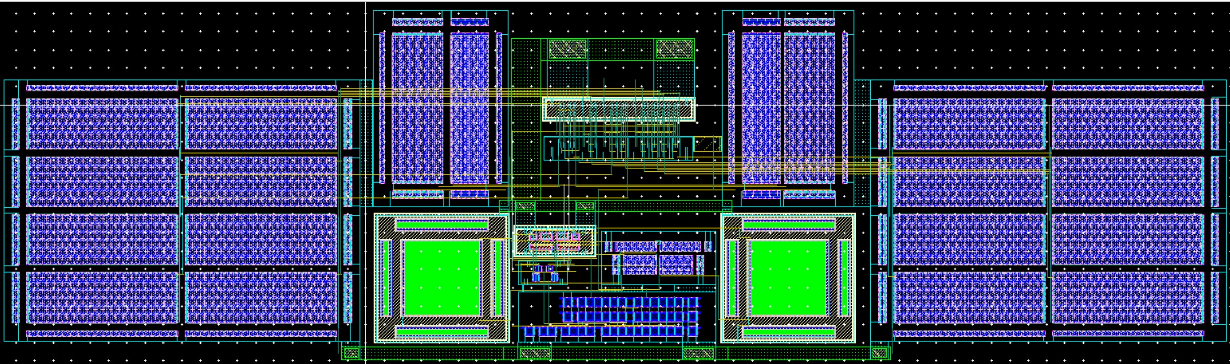
Figure 3: PGA Layout
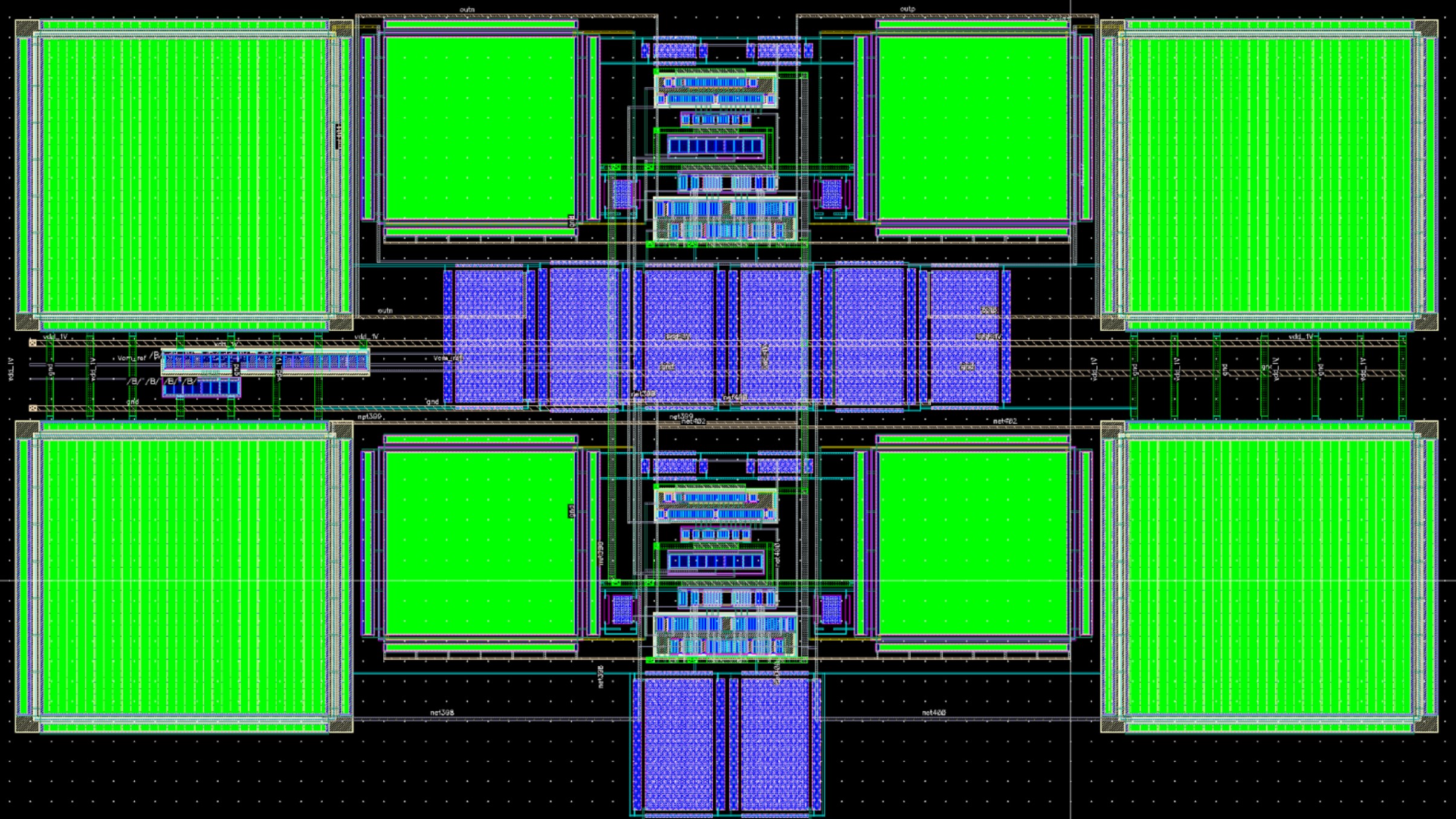
Figure 4: LPF Layout
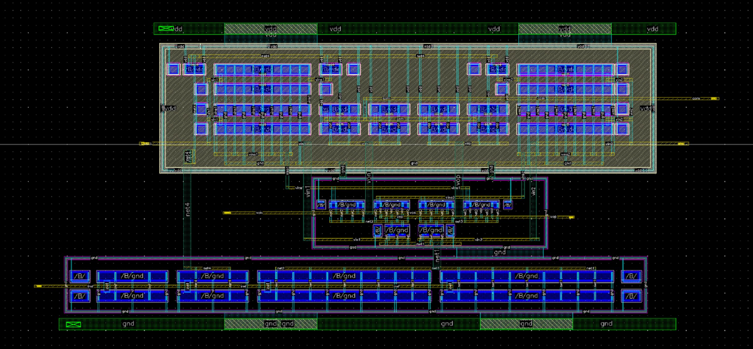
Figure 5: Gilbert Cell Layout
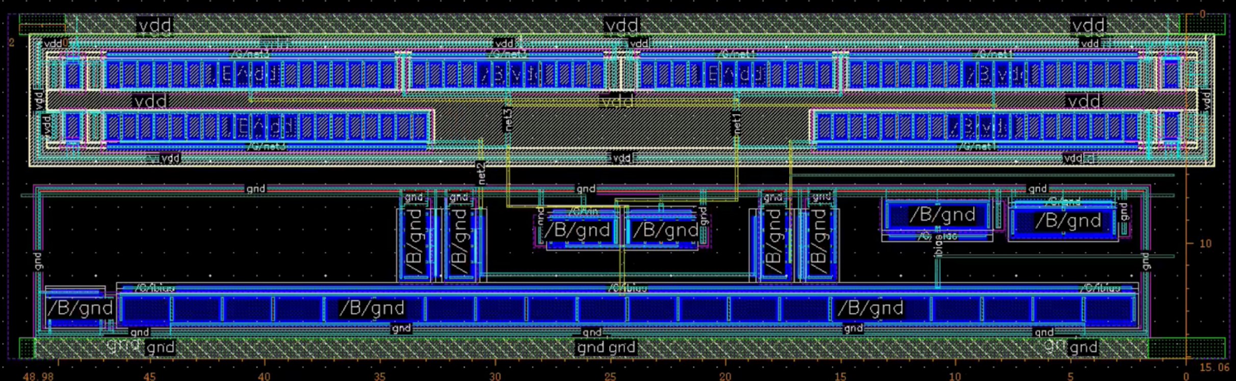
Figure 6: Comparator Layout
For the consistency of the full system layout we are using metal Layer M1 to M4 for the connection within the different blocks, M6 to M7 to connect the blocks, and M8 to M9 to connect to the pad frame.