IC Design
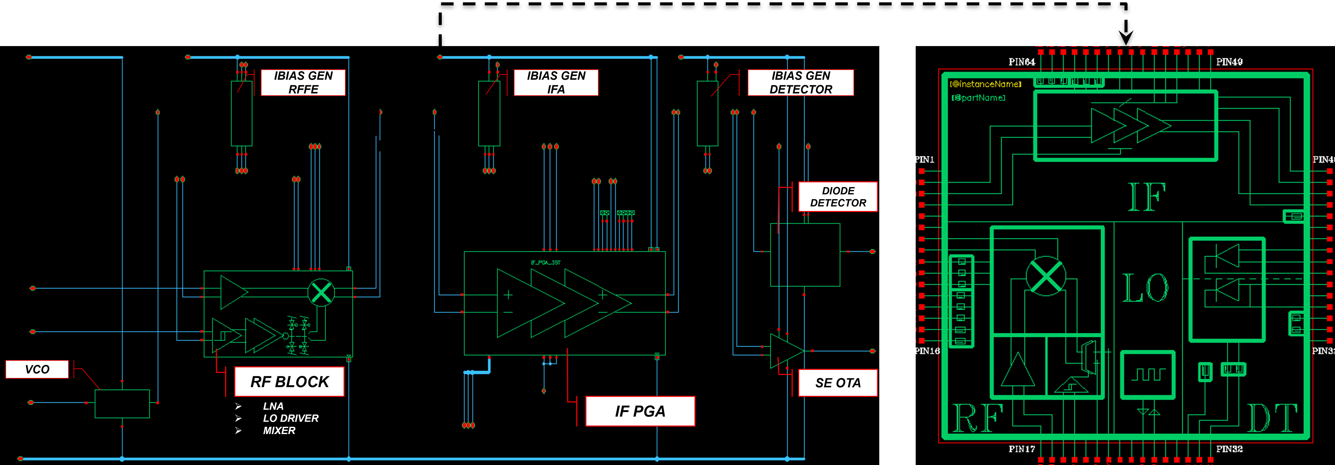
Welcome to our IC Design page, the core of our website. The top-level (cadence) schematic and symbol of the receiver is shown in Fig. 1 above. Here, we break down our circuit into four essential blocks: RFFE (LNA, Mixer, LO Driver), IFA (IF Amplifier), VCO, and Detector. Each plays a crucial role in capturing, amplifying, and demodulating AM signals. Explore our design methodologies and results as we guide you through the key components shaping the functionality of our AM Receiver.
1. RF FRONT-END (RFFE):
The LNA's primary role is to amplify the weak incoming signal from the antenna while adding as little noise to the system as possible. The LNA is a cascode amplifier defined by a common-source input stage feeding a common-gate output stage. The LNA is resistively loaded, this reduces the gain but improves the output noise when compared to alternative active load topologies. There is a common-mode load resistor at the output of the LNA, this is used to set the common-mode level of the output signal, which biases the RF port of the mixer, without overly increasing the gain prior to any filtering or channel selection. The LNA block diagram is shown in Fig. 2 below. The LNA schematic, annotated with key design parameters, is shown in Fig. 3 below.
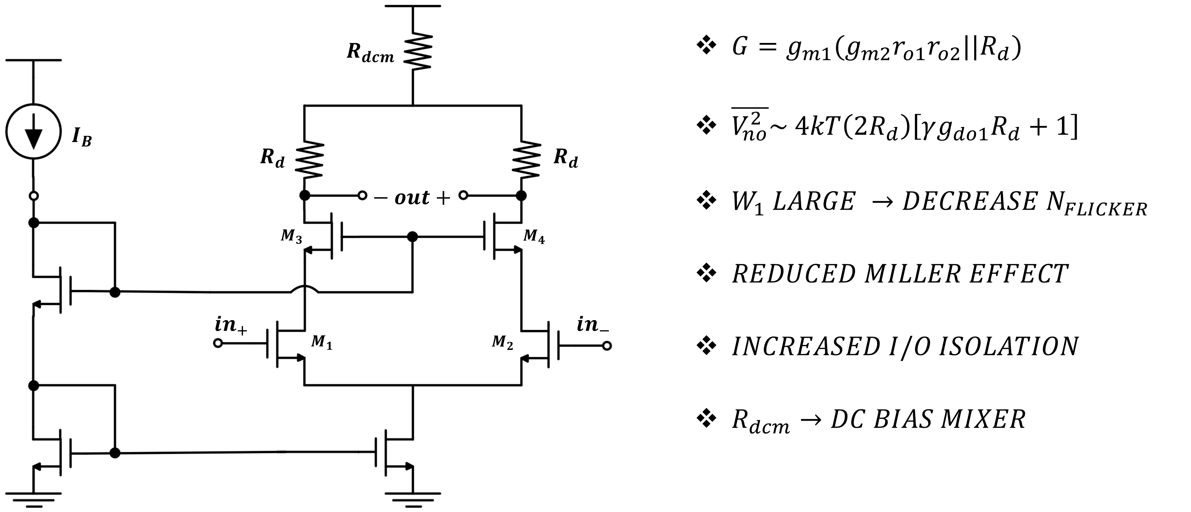
The gain is limited by Rd. A resistive load was chosen as oppossed to a cascode load because the gain from Rd was sufficient. The cascode topology was chosen primarly to reduce the miller effect and improve input-output isolation. At the AM input frequencies of operation, the dominant noise contribution was from the flicker noise of the differential pair transistors -- to minimize the flicker noise contribution the transistors were sized longer and consequently wider to achieve the designed performance
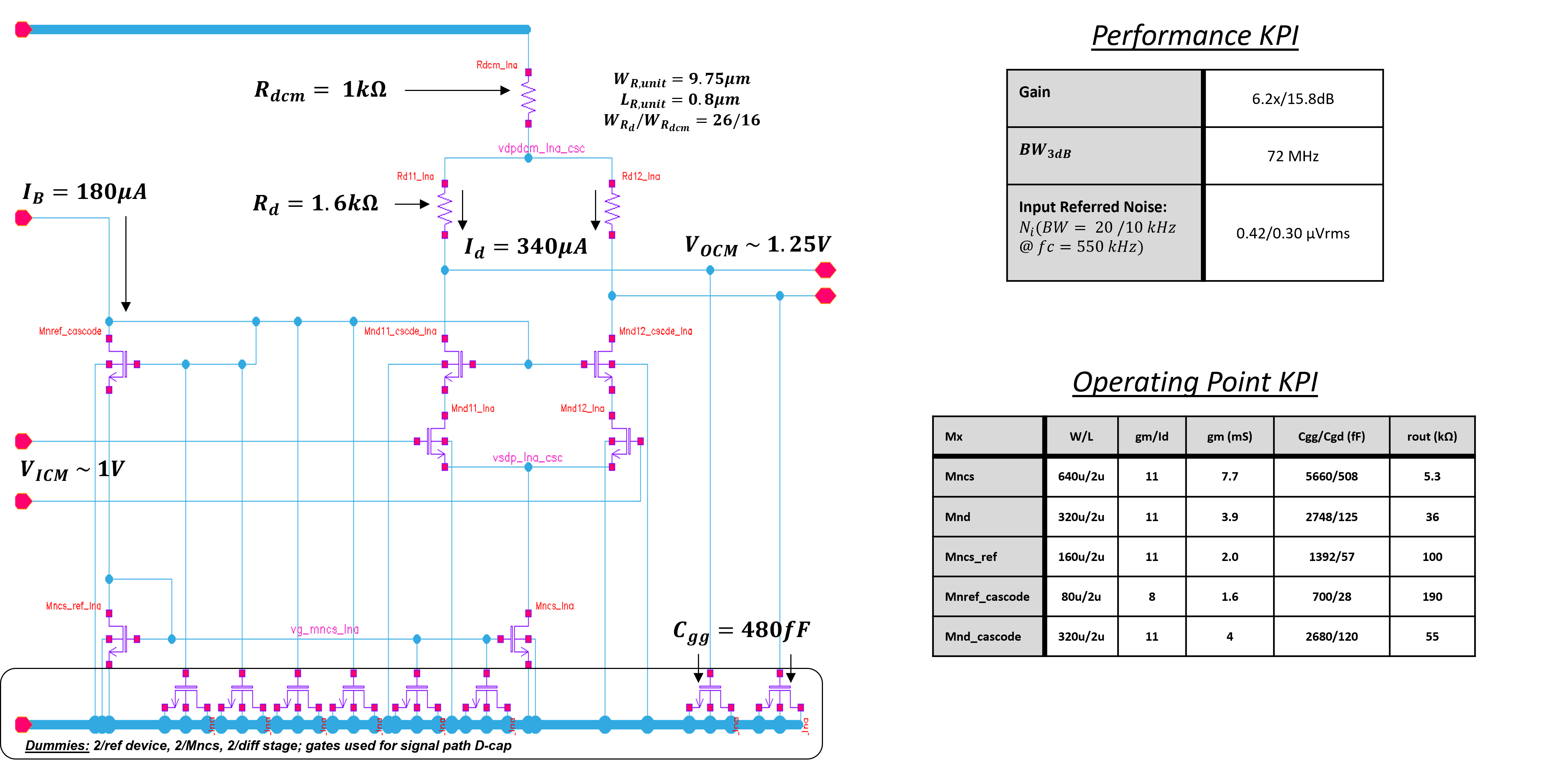
The cadence schematic with annotated design values, as well as performance and operating point KPI tables, are shown in Fig. 3 above. The performance was characterized through simulation results, which are shown in Fig. 4 below.
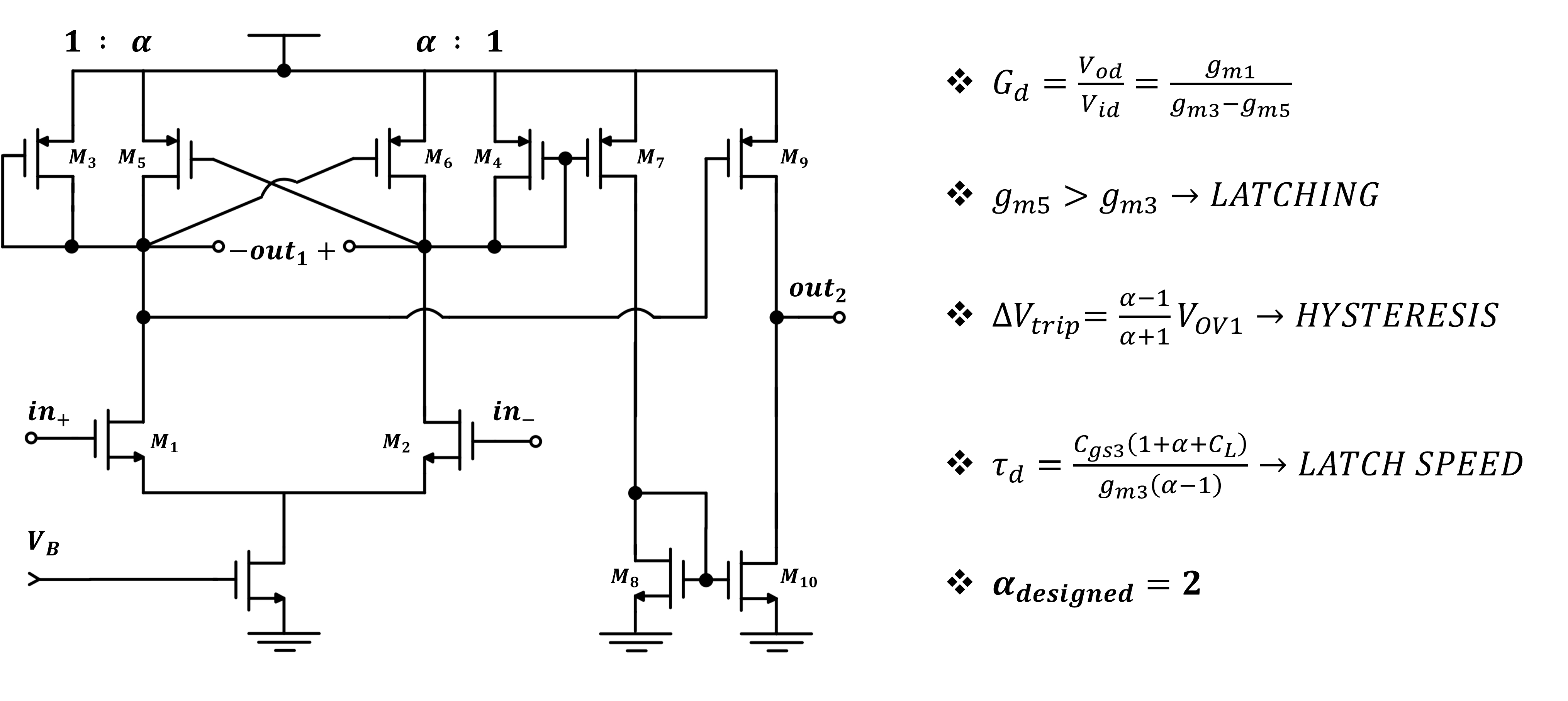
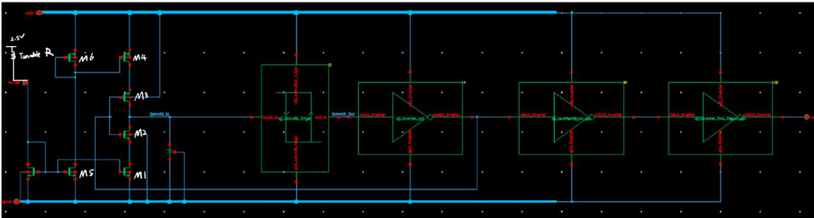
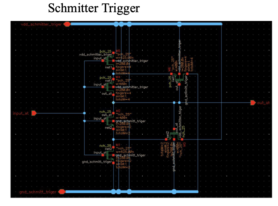
The primary role of the LO driver is to receive a single ended rail-to-rail signal, generated from either the on-chip VCO or off-chip, and convert it to a differential signal with a controllable amplitude and common-mode level. The first block in the LO driver is a schmitt-triggered buffer. The buffer hysteresis is used to improve the noise margins with respect to the received LO signal; this allows for successful reception from a wider range of input sources. The LO Driver block diagram is shown in Fig. 5 below. The schmitt-trigger schematic, annotated with key design parameters, is shown in Fig. 6 below.

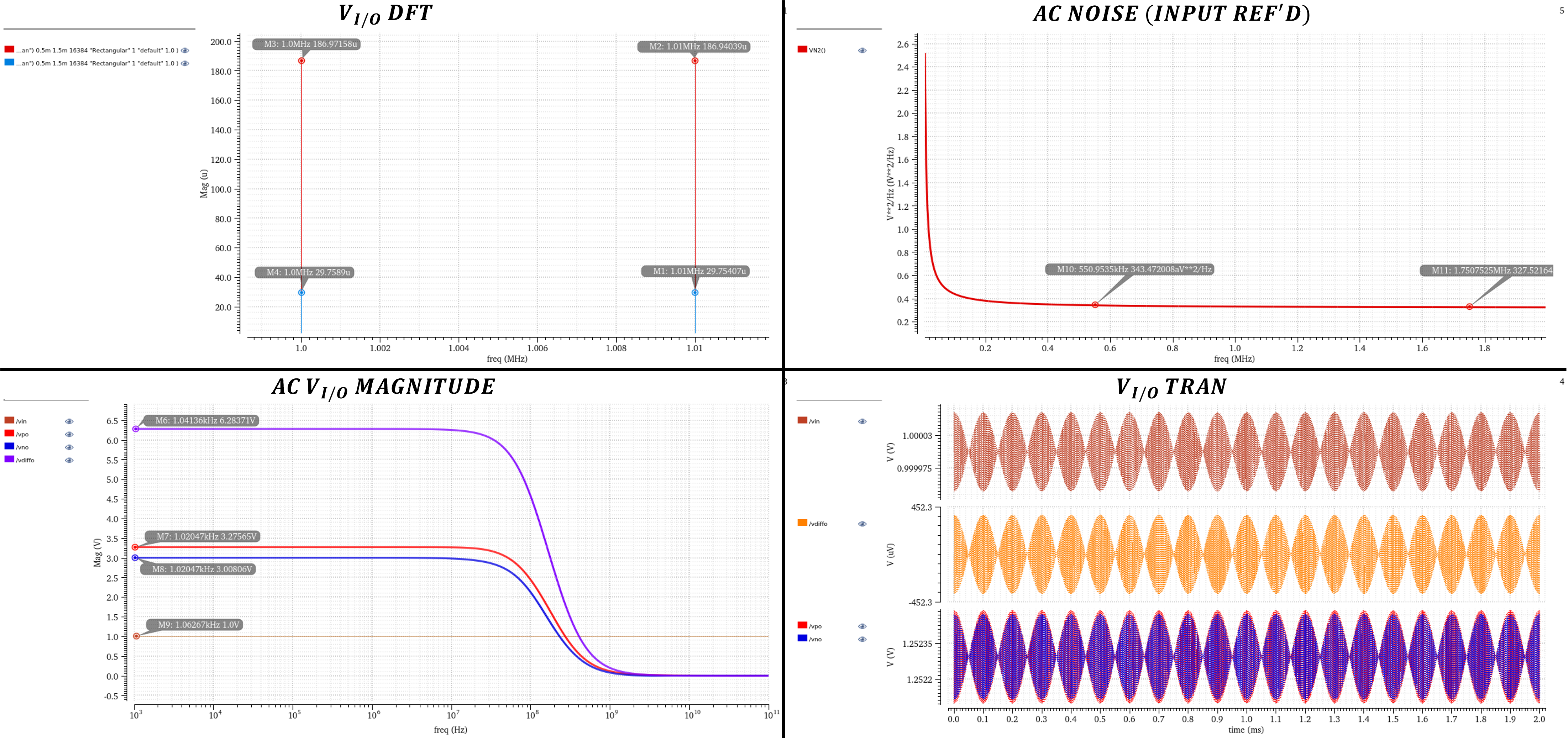
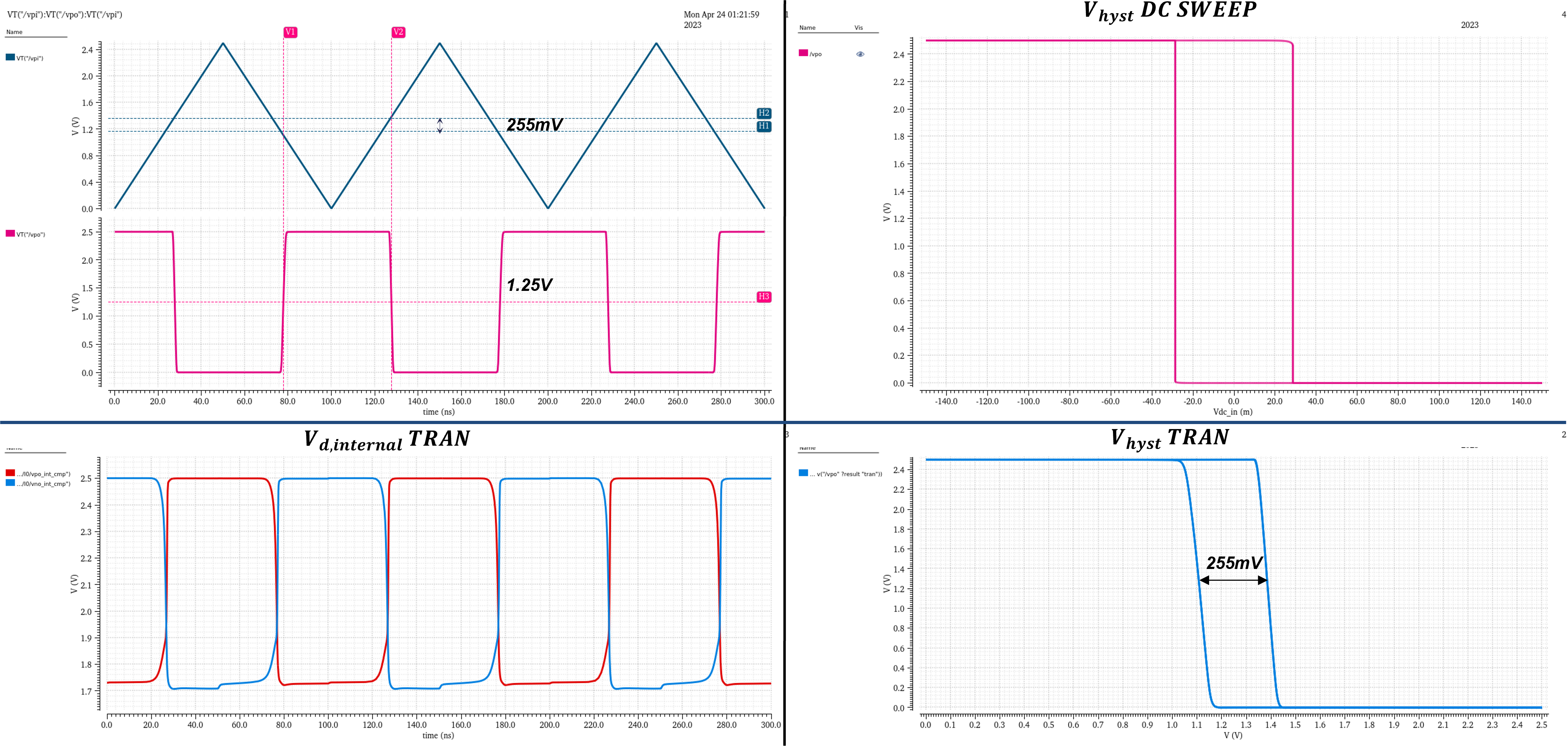
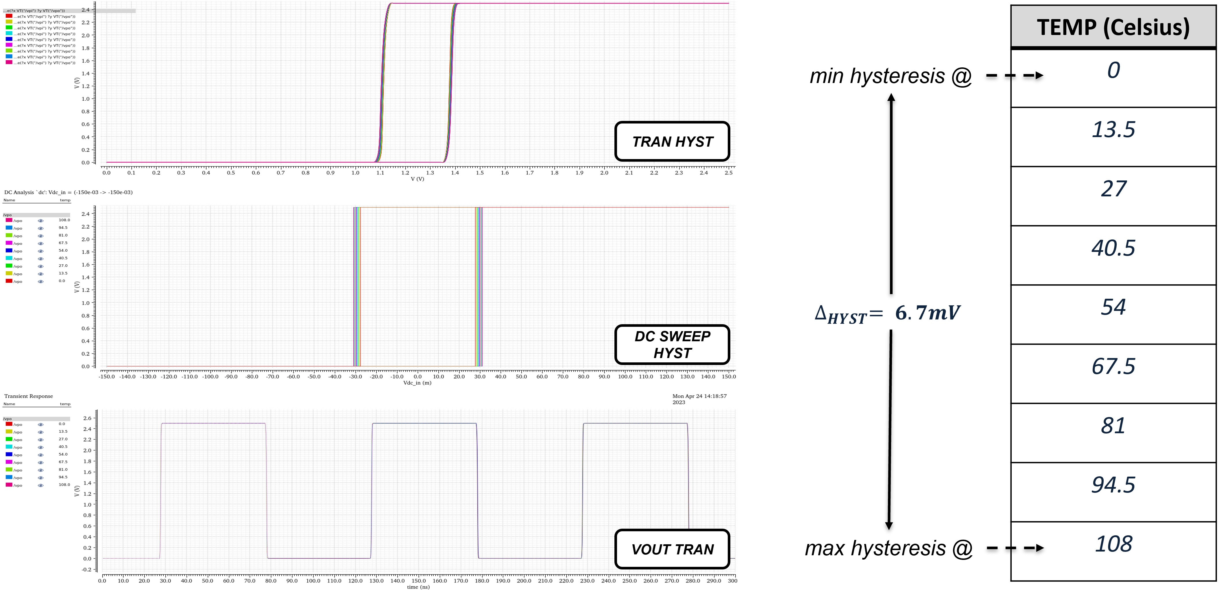
The performance was characterized through transient drain voltage waveforms, DC and transient hysteresis, and output waveforms shown in Fig. 7 below. The transient output and hysteresis responses were also characterized across temperature, displayed in Fig. 8 below. All simulation results were generated in Cadence.
The mixer performs the frequency up-conversion from the desired AM channel up to the intermediate-frequency of 10.7MHz. The mixer has two differential input ports, one for the RF signal and one for the LO signal. No channel selection or filtering proceeds the mixer, thus there is the potential for large in-band and out-of-band blockers present at the mixer input. Consequently, linearity with respect to the desired output IF signal was the primary constraint during the mixer design process. The mixer schematic architecture, along with annotated key design considerations, are shown in Fig. 9 below.
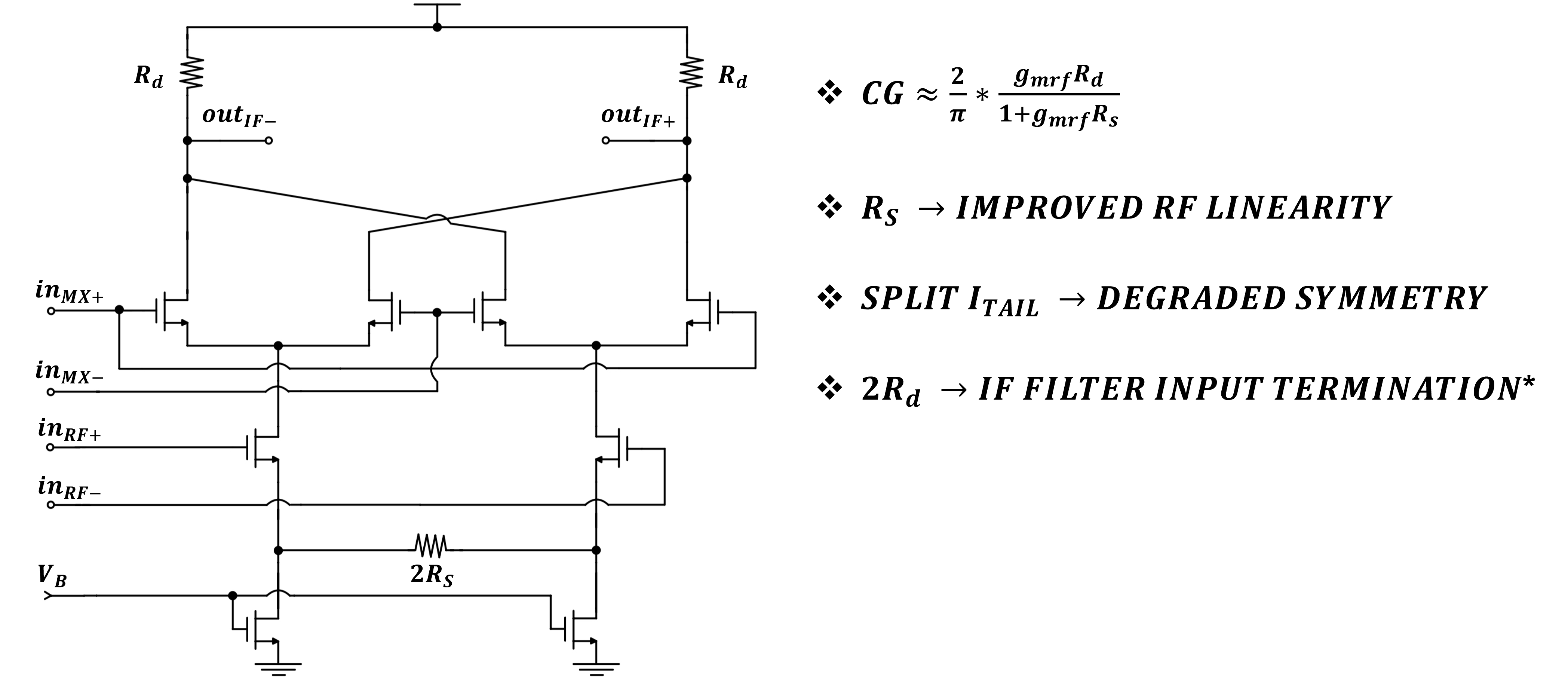
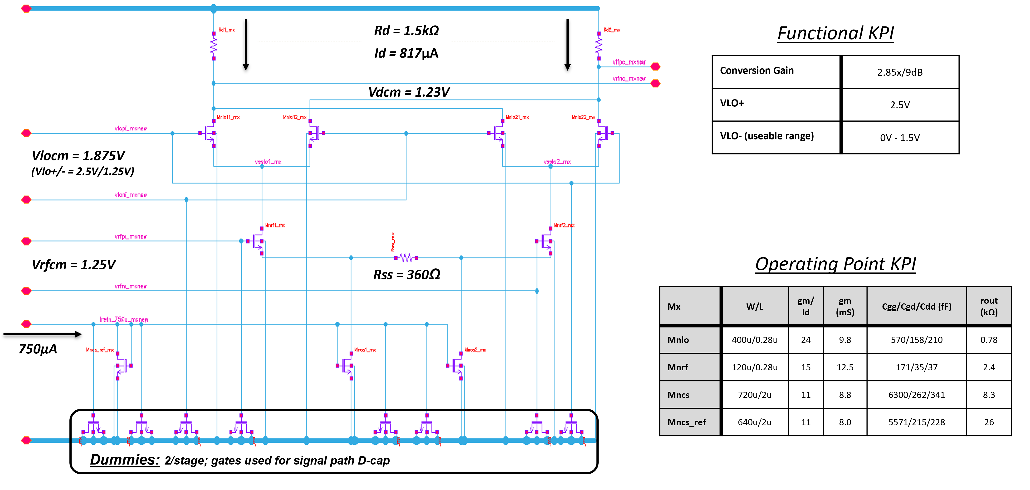
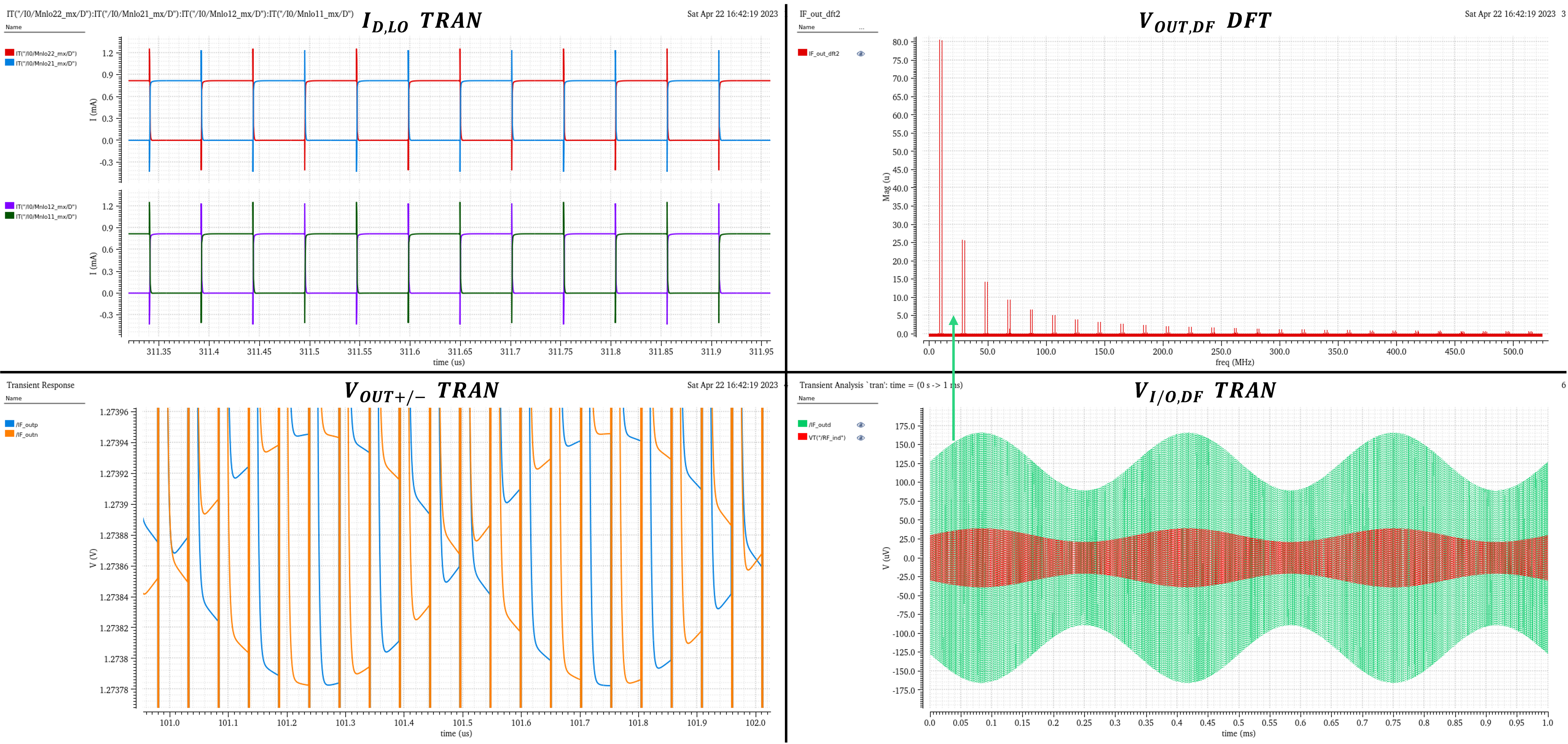
The cadence schematic with annotated key design considerations, as well as performance and operating point KPI tables, are shown in Fig. 10 below. The performance was characterized through simulation results done in Cadence, which are shown in Fig. 11 below.
2. Intermediate-Frequency Amplifier (IFA):
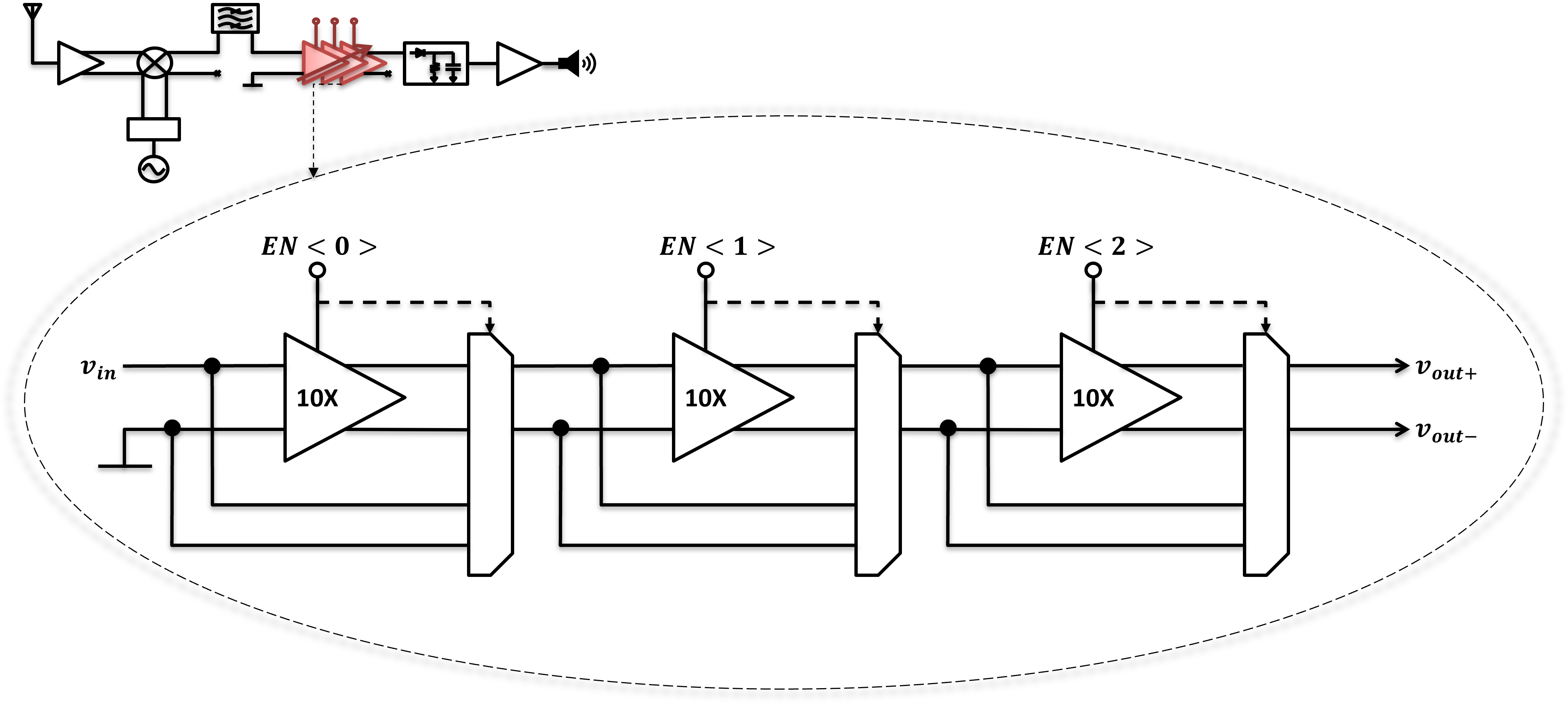
The intermediate-frequency amplifier (IFA) amplifies the selected AM channel that has been upconverted to the IF frequency of 10.7MHz. Variable gain is implemented to accomodate a wide range of input signal levels and thus improve the dynamic range of the system. The block diagram of the three-stage amplifier is shown in Fig. 12 below. The variable gain is implemented through differential muxs that succeed each individual amplifier. The signal that passes to the output is chosen through the combination of three enable bits, allowing for gains of 1x, 10x, 100x, or 1000x. The single-stage architecture is shown in Fig. 13 below. The first of the three stages has different external resistor values to accomodate the output termination (resistive) requirement of the IF Filter (3k). The second and third stage use larger resistors to improve the open loop gain by reducing the loading at the outputs. This is possible because the second and third stages do not load the output of the IF Filter.
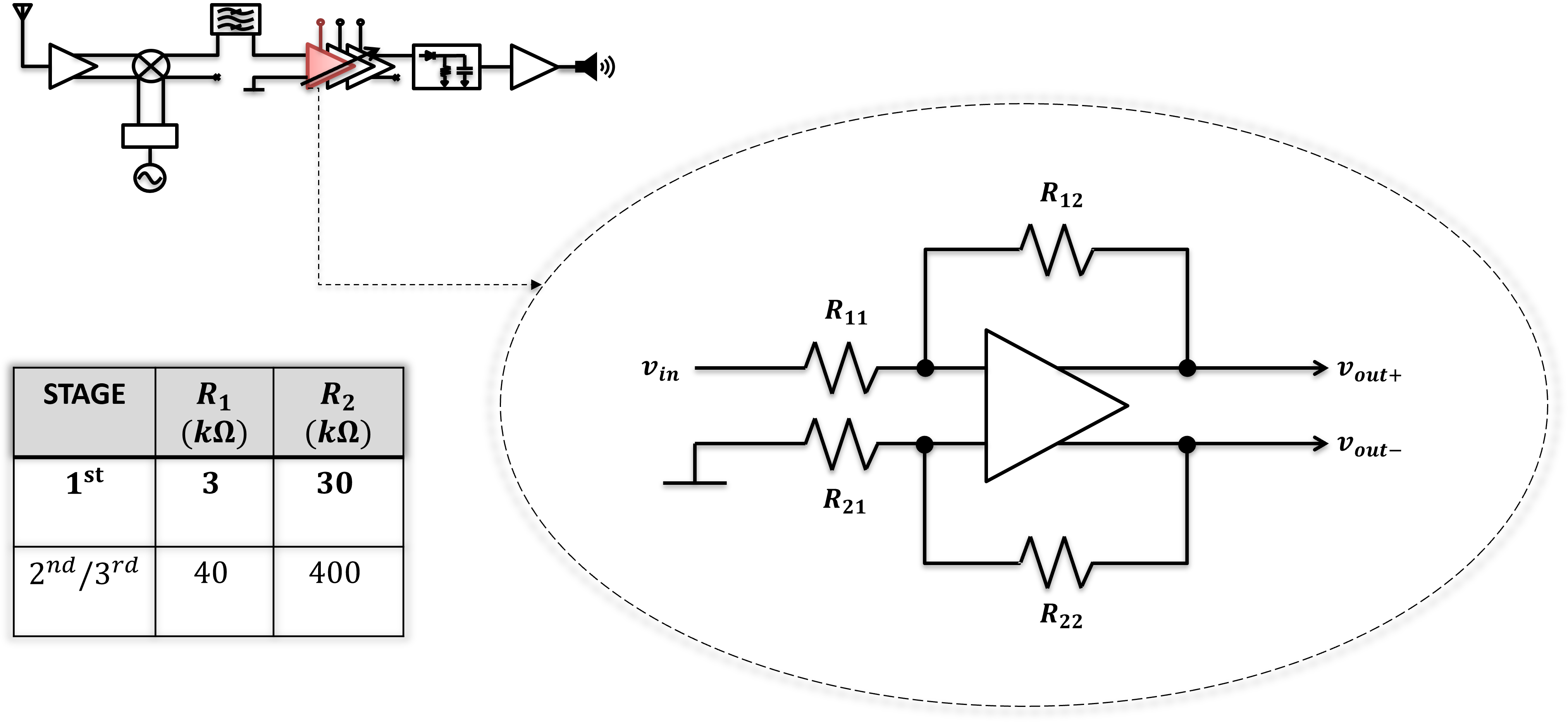
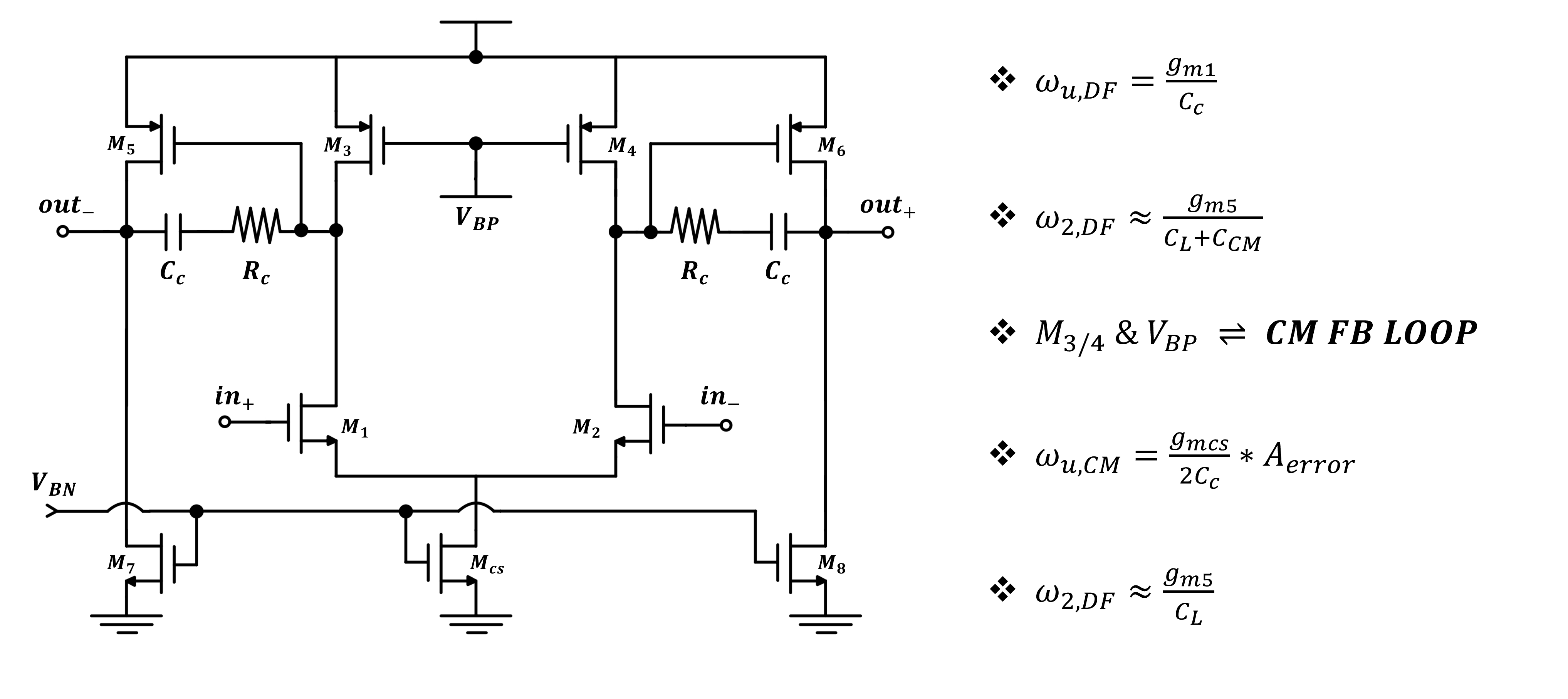
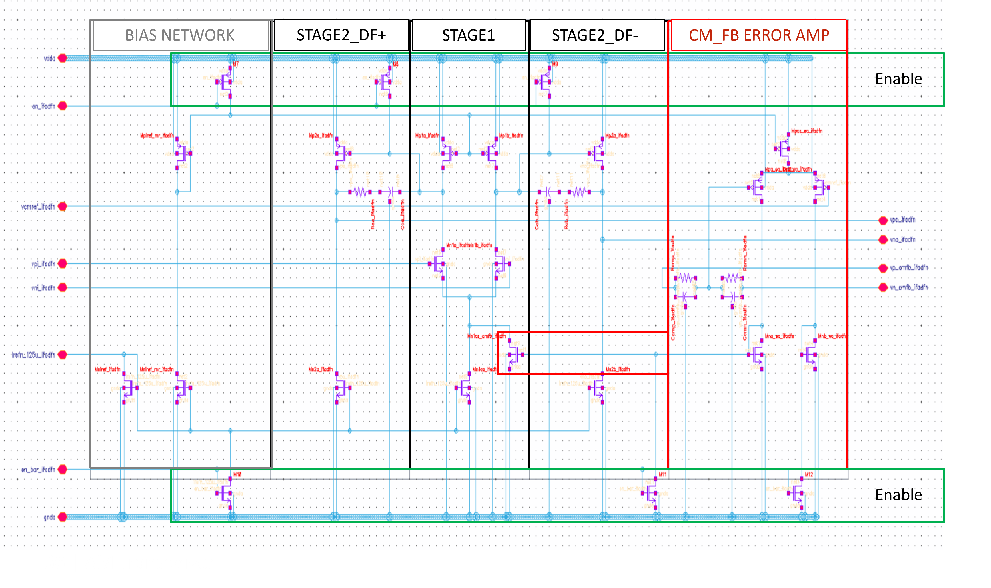
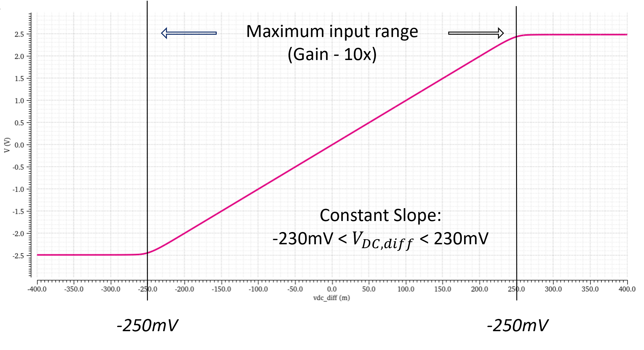
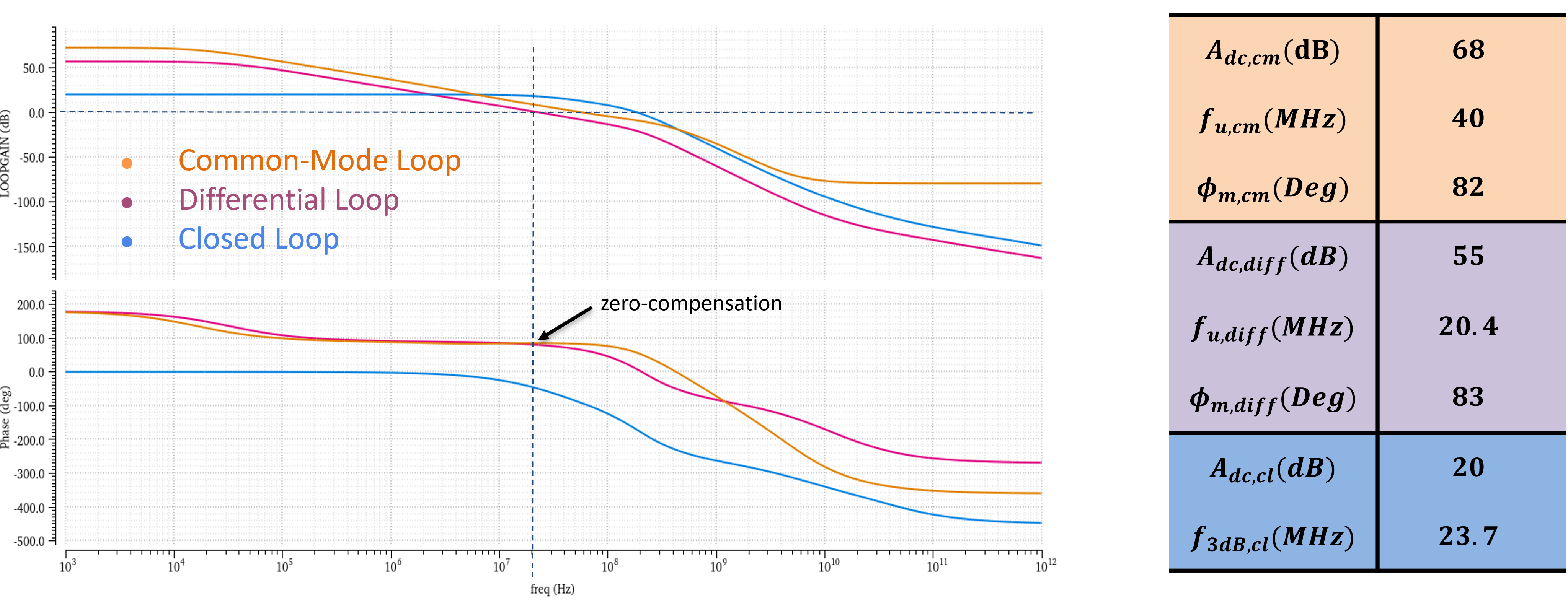
The single-stage core OTA schematic architecture with annotated key design considerations, are shown in Fig. 14 below. The full cadence schemmatic with highlighted stages, including the common-mode feedback circuitry,are shown in Fig. 15 below. The single-stage performance was characterized through DC and frequency domain (stability) simulation results done in Cadence, which are shown in Fig. 16 and Fig. 17 below.
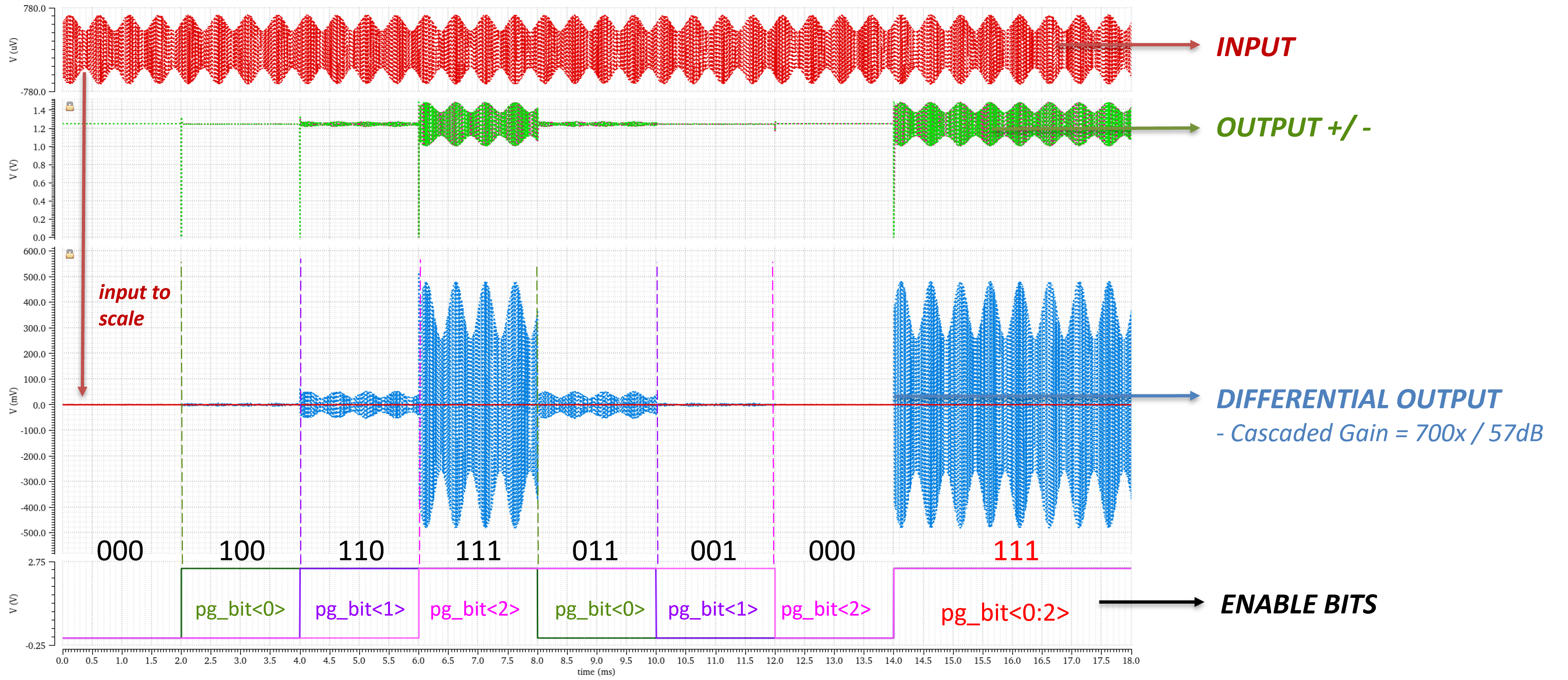
The three-stage IFA transient waveforms, annotated with their respective measurement points in the signal chain, are shown above the time-corresponding gain control sequence (enable bits) in Fig. 18 below.
3. VCO Block:
Voltage-Controlled Oscillator (VCO):
At the heart of variable frequency signal generation is the voltage controlled oscillator (VCO). It's main function is to output a controllable square wave signal and output it to the Mixer.
The Control Block:
The left side of VCO, The core of VCO operation is to manipulate the resistor value to change the bias current and change the charging speed through the capacitor, adjusting its output frequency.
1. When output is high, switch M3 is off and switch M2 is on; current source M1 discharges capacitor C; once the capacitor voltage reaches the comparator trigger, the output goes low.
2. When output is low, switch M2 is off and switch M3 is on; current source M4 charges capacitor C; once the capacitor voltage reaches the comparator trigger, the output goes high.
3. The voltage on the capacitor is a triangle-wave with an amplitude determined by the hysteresis in the comparator (Schmitt trigger).
4. M5/M6 make sure that the charging current through M4 is the same as the discharging current through M1.
The Schmitt Trigger Block:
Converts the triangle wave generated on the left into a square wave.
Buffer Block:
We used three inverters as a buffer. This section acts as the final stage, ensuring that the signal maintains its integrity as it leaves the VCO. Protect the signal from any external interference that could degrade its quality.
4. Detector Block:

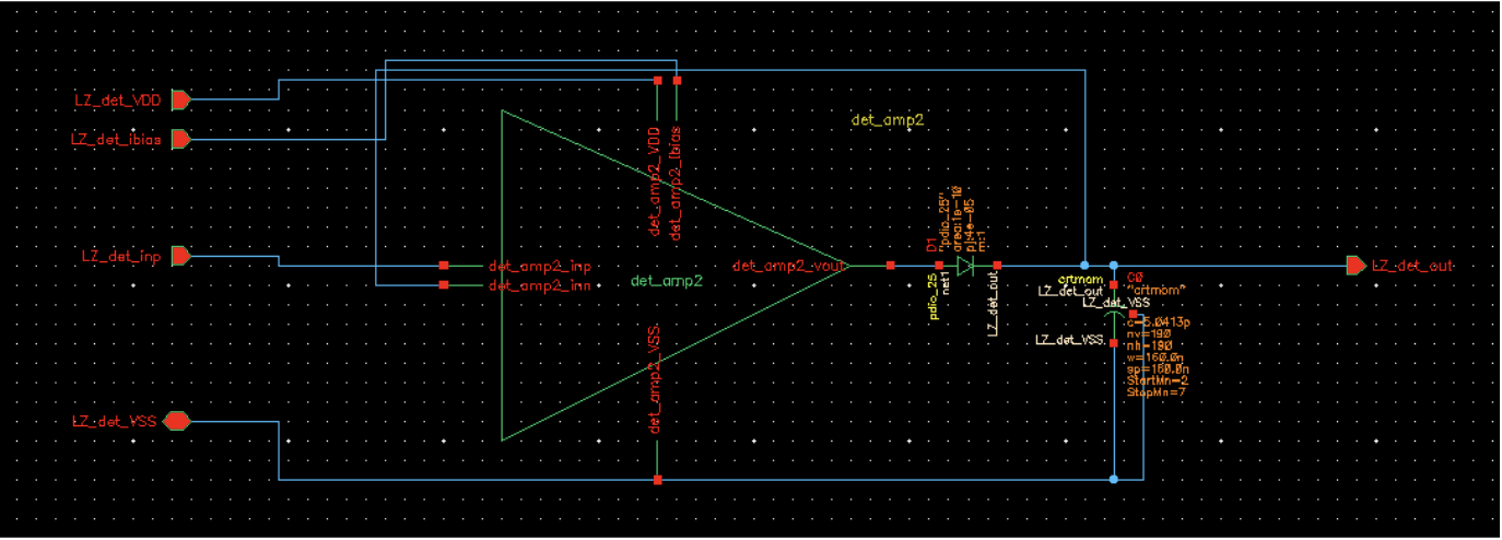
This active envelope detector is based on an envelope detector which is a practical detector that uses a diode, capacitor and resistor between the input and the output to provide an output which is the envelope of the input signal. With all envelopes of the high-frequency input signal detected, we can recover the message signal which was mixed with carrier frequency before. And the output message signal will be sent to the audio power amplifier.
By choosing the correct capacitor and resistor, according to the equation “1/fcarrier < RC < 1/fmessage", this active envelope detector can detect a wide range of the 100Hz to 4 kHz input message signal. A low pass filter is added after the parallel resistor and capacitor pair to get rid of the high frequency noise so the output signal will be more smooth. In addition, by adding an op-amp to the basic envelope detector, this detector can be more sensitive to the edge of the input signal. This specially designed op-amp can work at very high frequencies, even over 11 MHz, with enough gain and the phase margin is about 80 degrees to make it stable. With the help of active design, this detector can keep enough gain with high frequency input signal.
In the detector, the parallel resistor and capacitor pair are big, which will take a lot of space on chip, so we decided to make those capacitors and resistors off-chip.
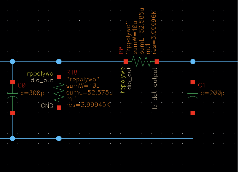
Here are on-chip parts, which are detector amplifier, diode, and one on-chip capacitor.
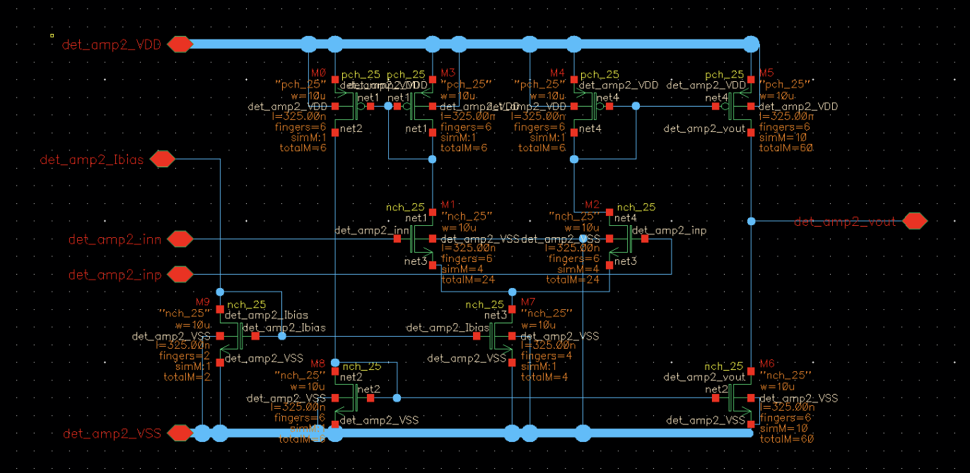
Here is the design of the detector amplifier with details. There are four PMOS devices and six NMOS devices.
5. Biasing Block:
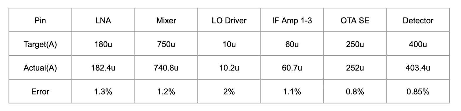
We incorporated an on-chip current biasing system utilizing current mirror design. This system efficiently provides currents to three essential on-chip blocks, namely RF, IF, and Detector blocks.
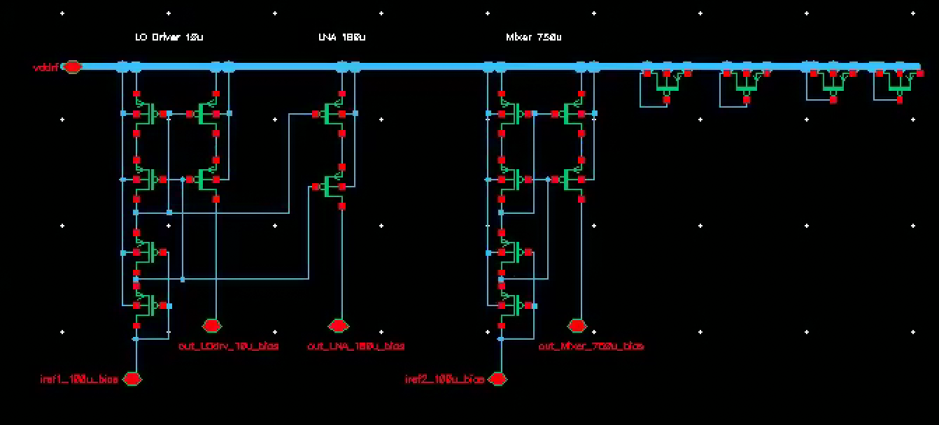
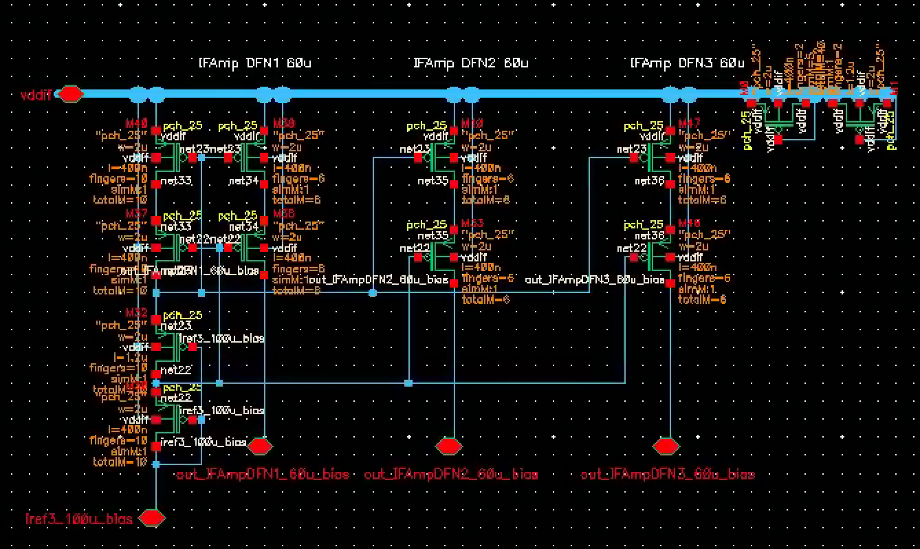
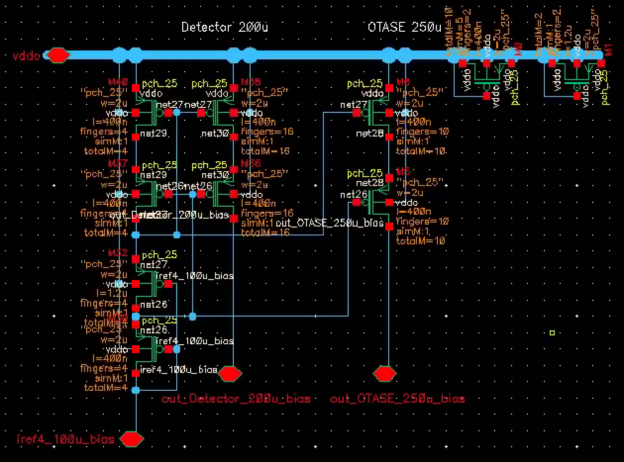
The biasing blocks, operating separately, deliver 6 distinct current values within the range of 10uA to 750uA. Achieving this involved meticulous design decisions, particularly in sizing transistors, to ensure optimal performance and functionality.