
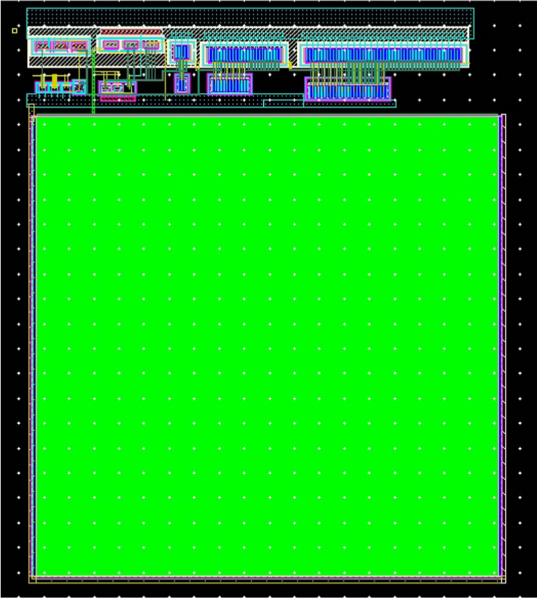
IC Layout
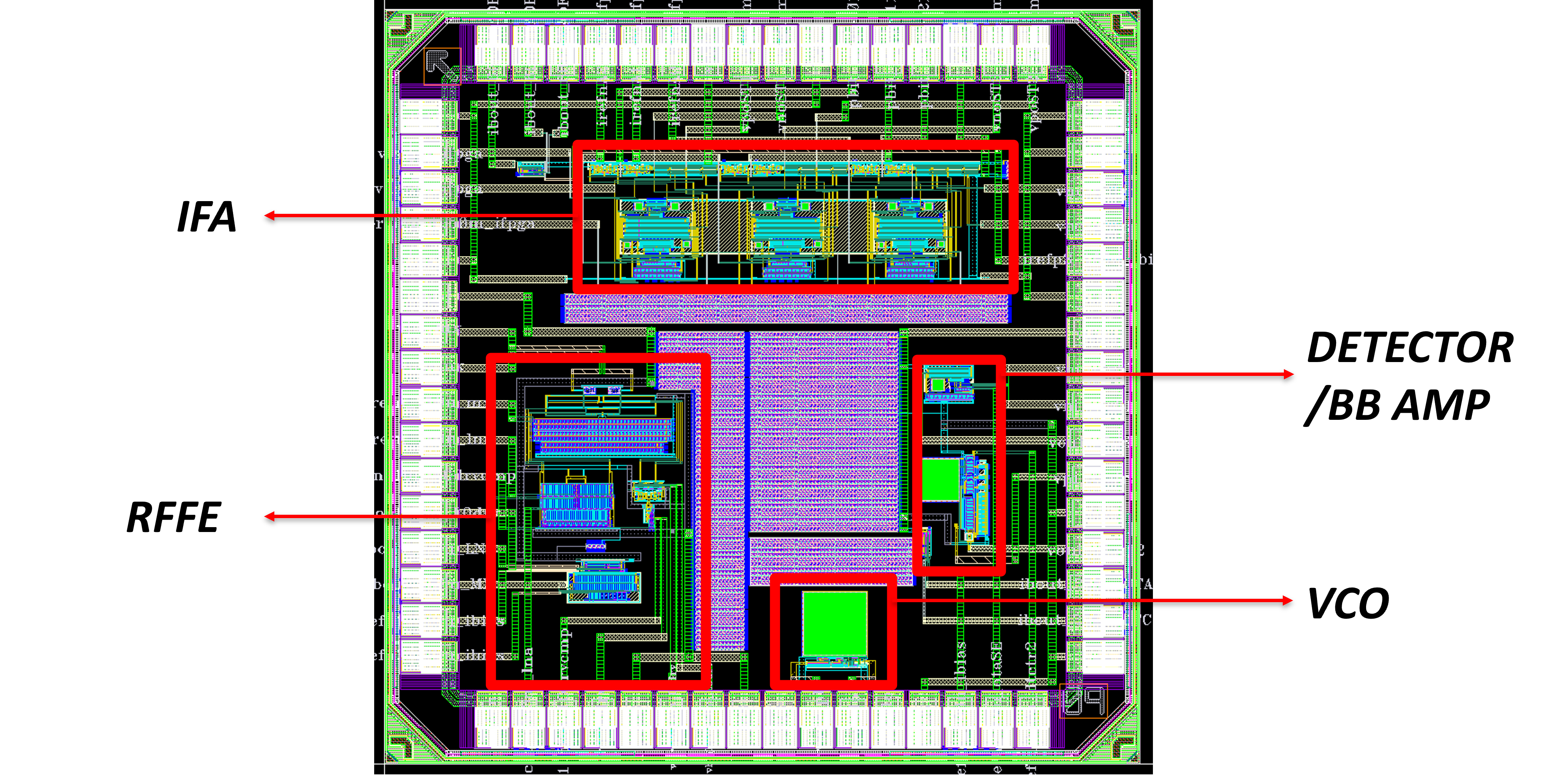
The overall Chip Layout is shown above.
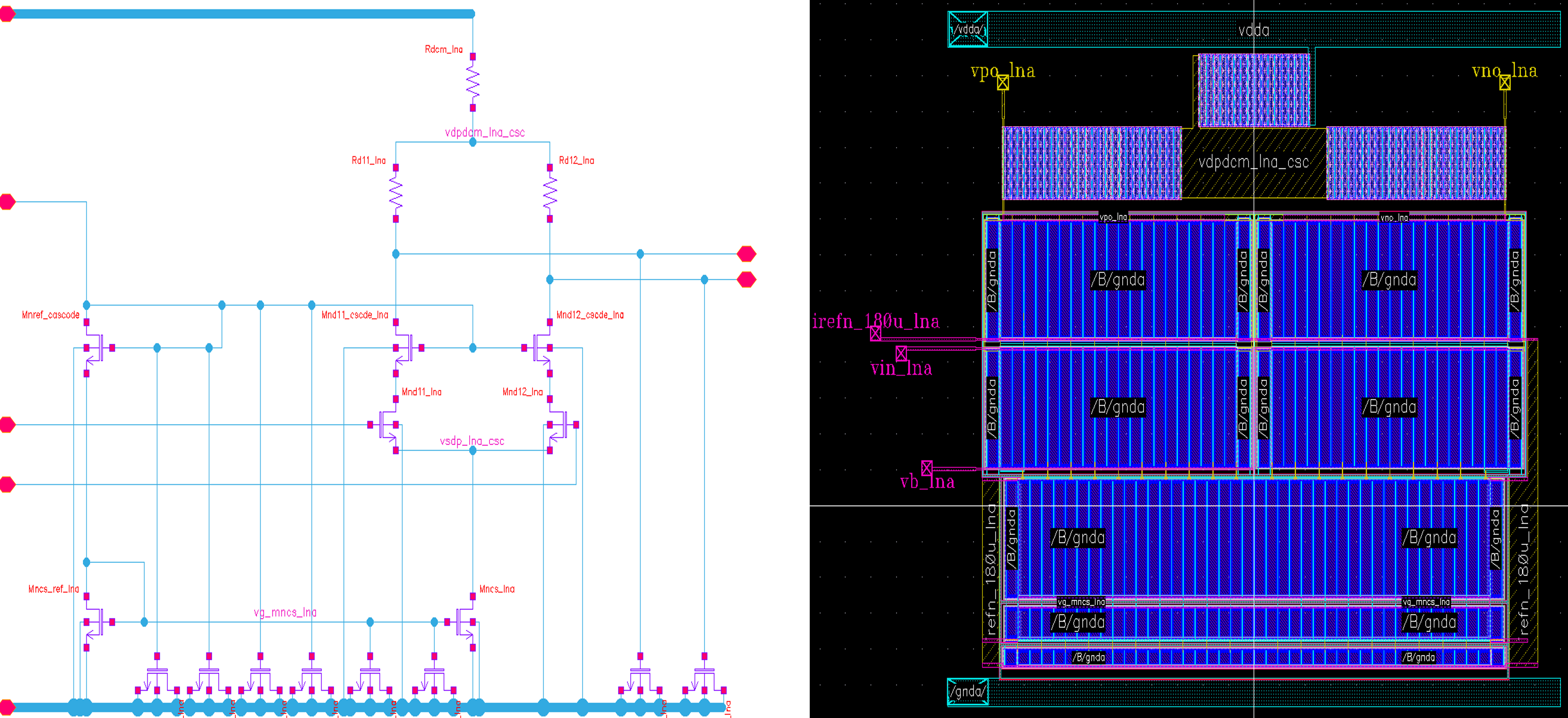
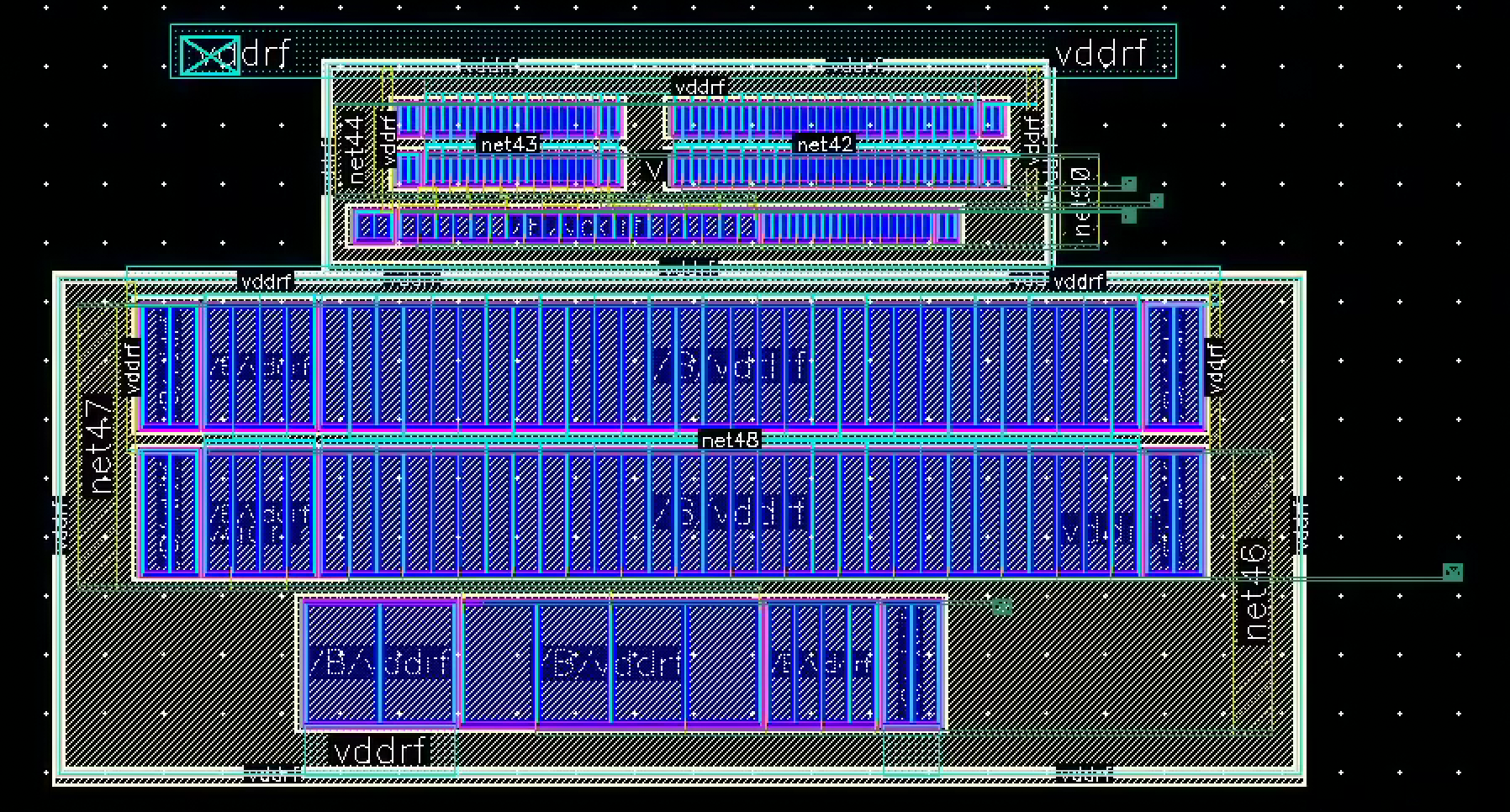
RF FRONT-END (RFFE) LAYOUT:
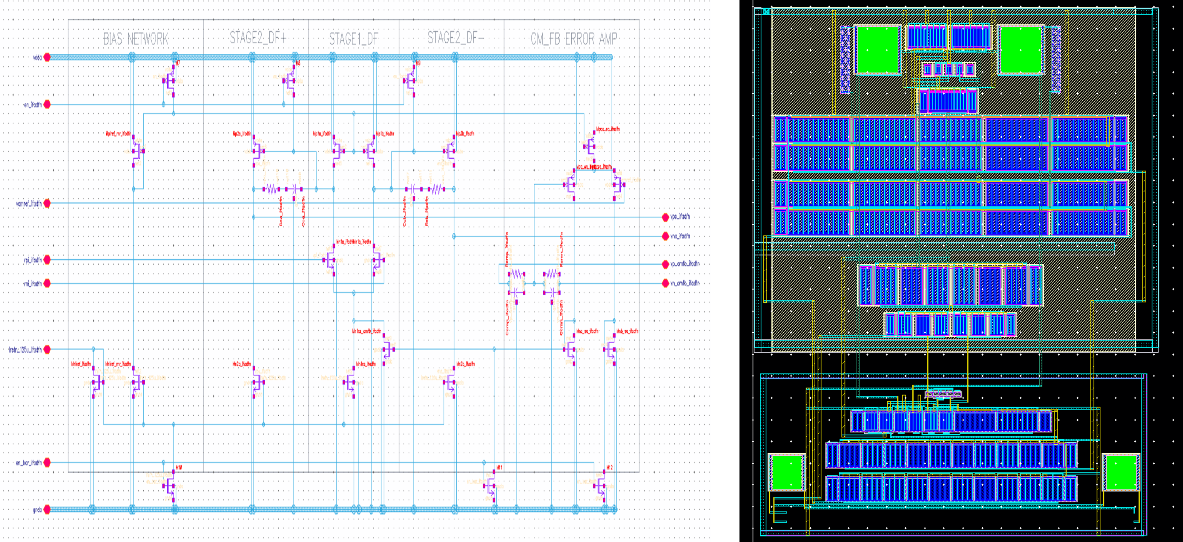
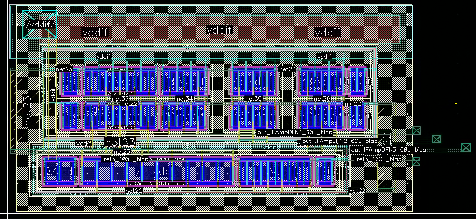
IF AMPLIFIER (IFA) LAYOUT:
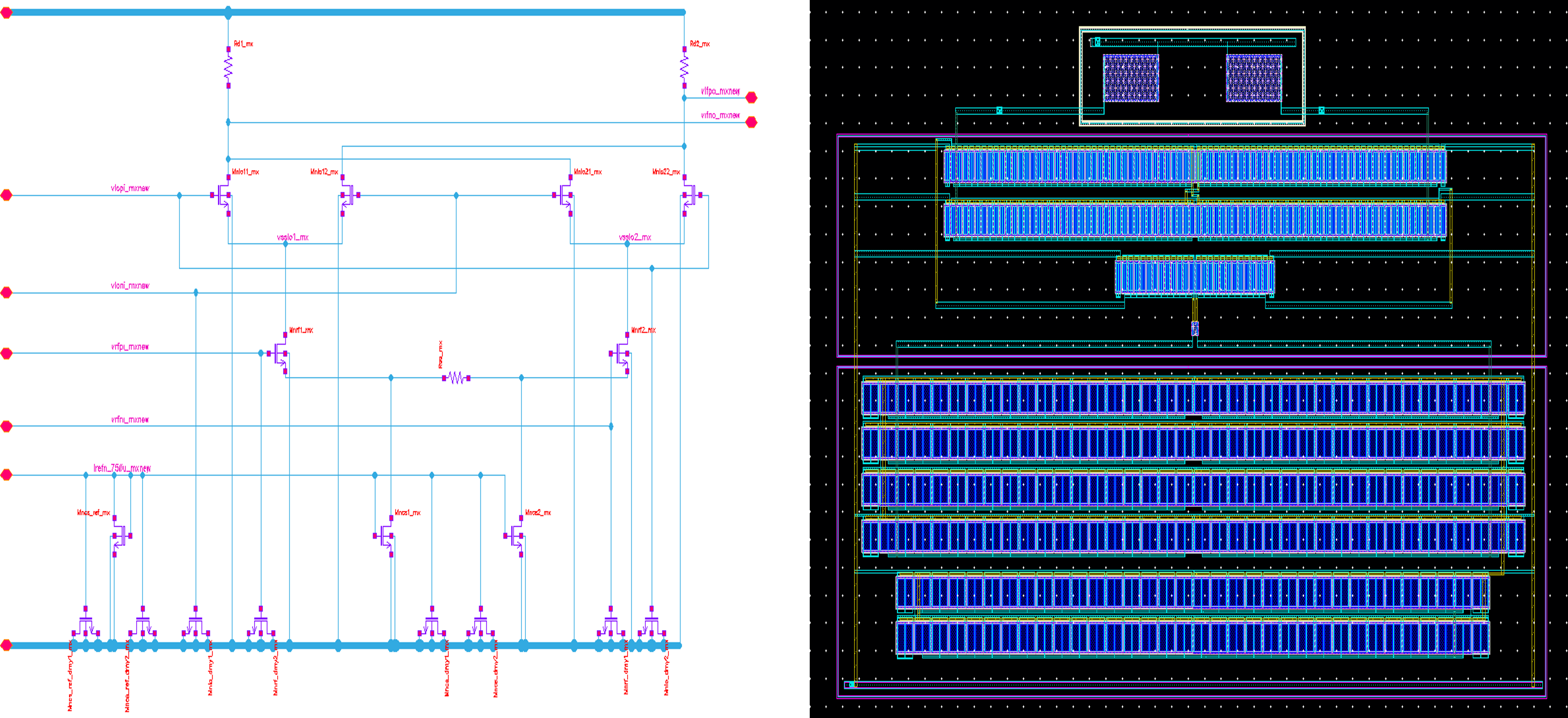
VCO Block:
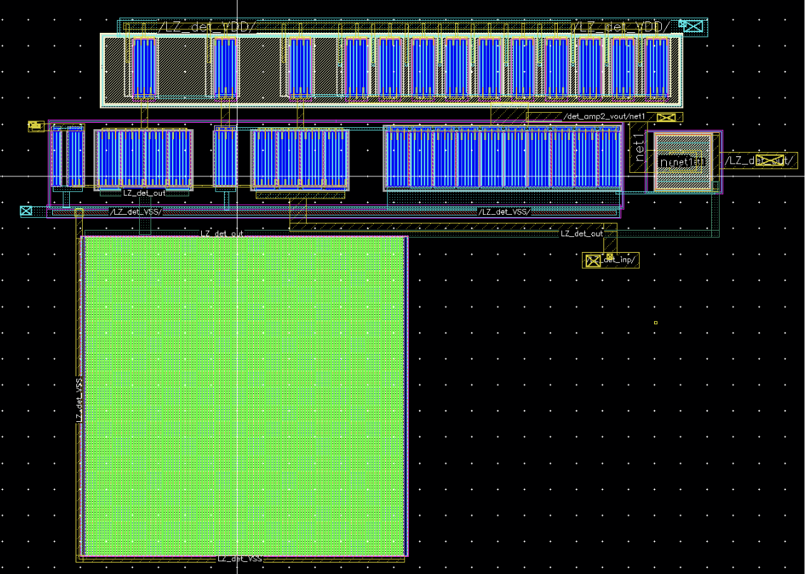
Detector Block :
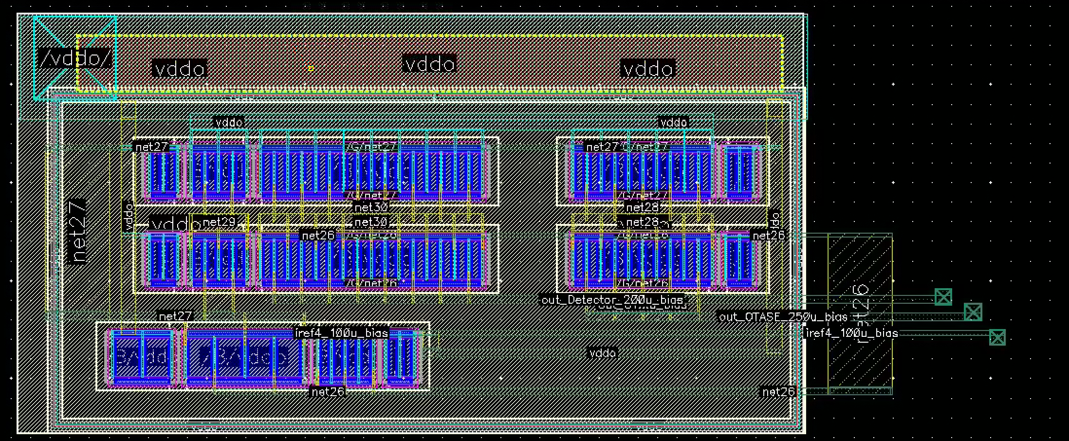
Biasing Block :
The overall Chip Layout is shown above.
RF FRONT-END (RFFE) LAYOUT:
IF AMPLIFIER (IFA) LAYOUT:
VCO Block:
Detector Block :
Biasing Block :