PCB Design
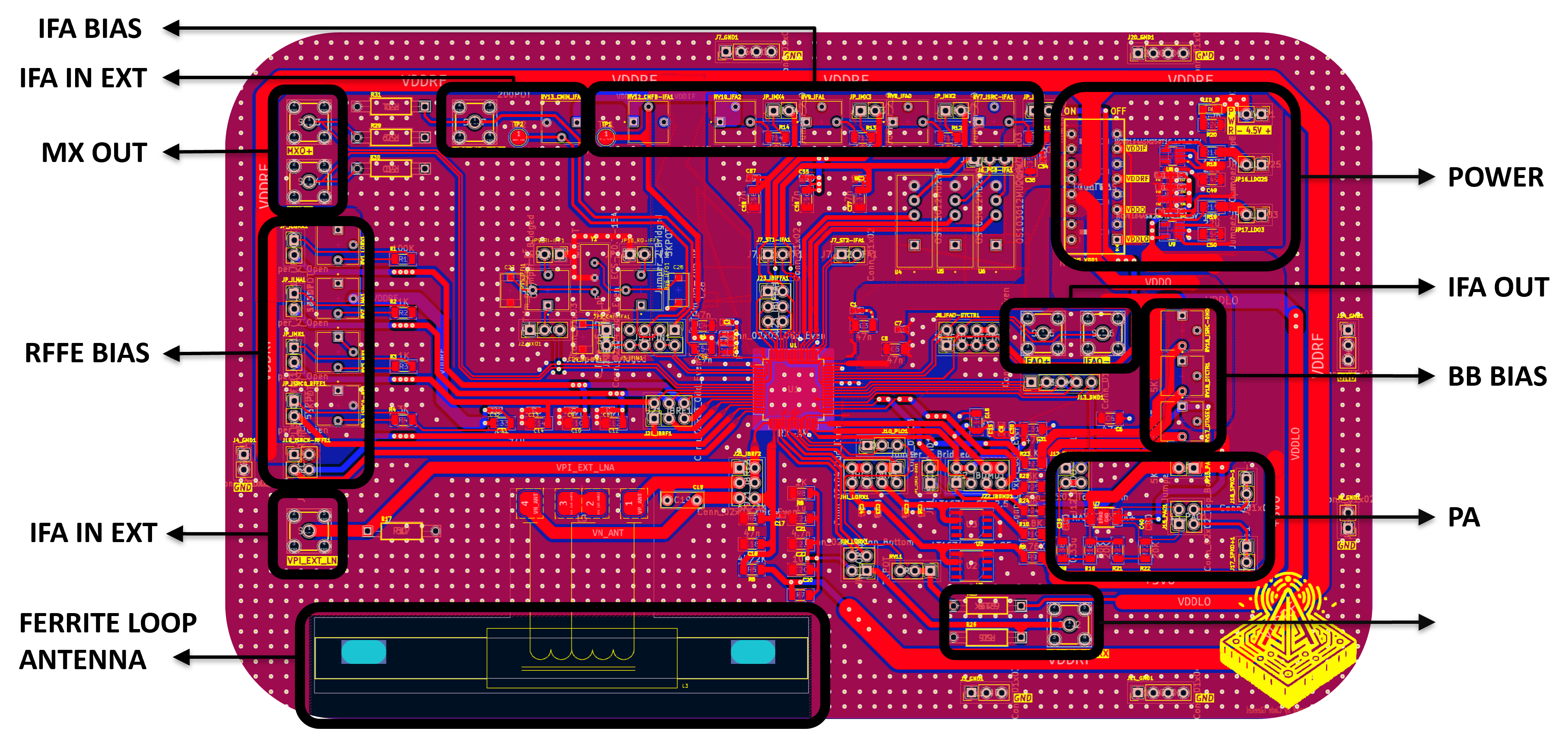
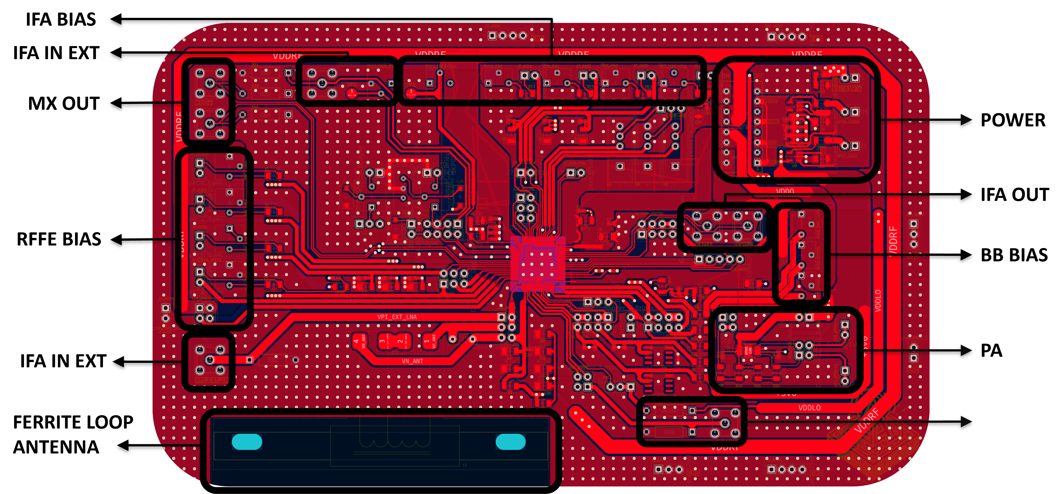
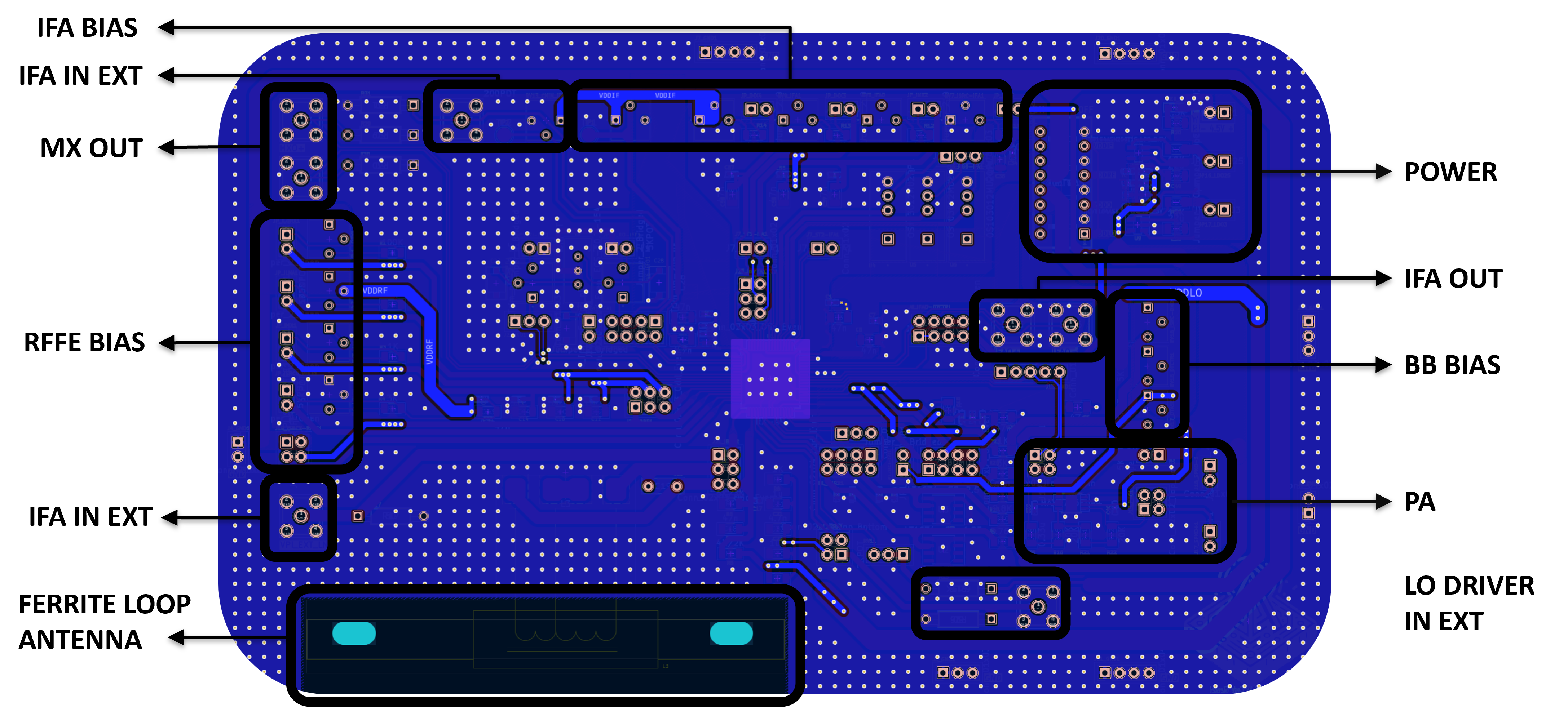
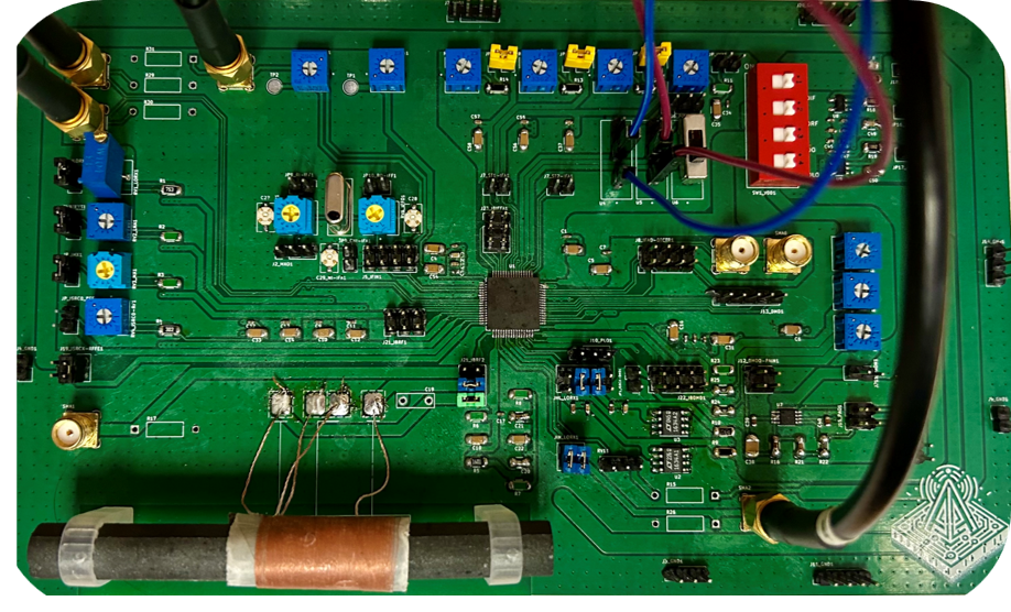
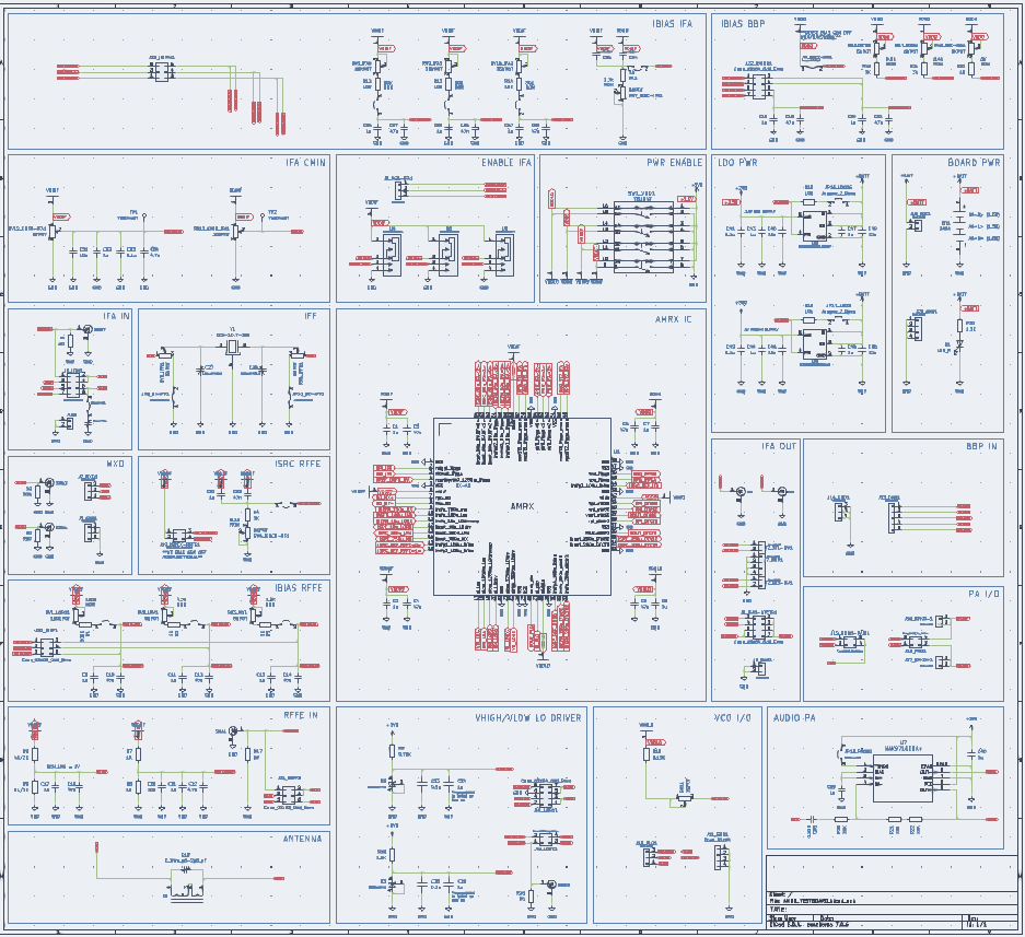
The PCB was designed using KiCad. The primary goal of the PCB is to provide independent biasing options to all subsections on-chip, and to provide a selection of input source and output load options to each subblock. The options allow for integrated system configuration, as well as independent testing of each subblock. Ease and simplicity of system integration was traded for a more robust and flexible design with respect to testing, debugging, and application. An antenna is integrated and fastened to the front of the PCB, and the PCB was designed to run off three AA batteries, for the potential use as an independent portable AM radio module once complete system level integration is achieved. The final PCB, with SMA connectors attached during the testing process, is shown above in Fig. 1.
PCB SCHEMATIC
PCB LAYOUT