
Testing
This section documents the current testing progress of the AMRX and its sub-blocks. Due to PCB manufacturing delays, the majority of the testing documented in this section was done on a breadboard using a socket and and universal expansion surfboard that allowed all groups to initially test their chip on a breadboard (The surfboard was designed by a member of this group). Consequently most testing to date has been sub-block functionality characterization. However, testing remains on-going; please check back later for a more complete documentation of measured performance metrics on full system-level test results.
System-Level Testing Results
This subsection documents our two most complete system-level testing results to date. The tests are categorized into the following two groups:- 1. Transmitter configured demonstration of complete internal signal path.
- 2. RFFE reception of on-air AM radio channel from antenna.
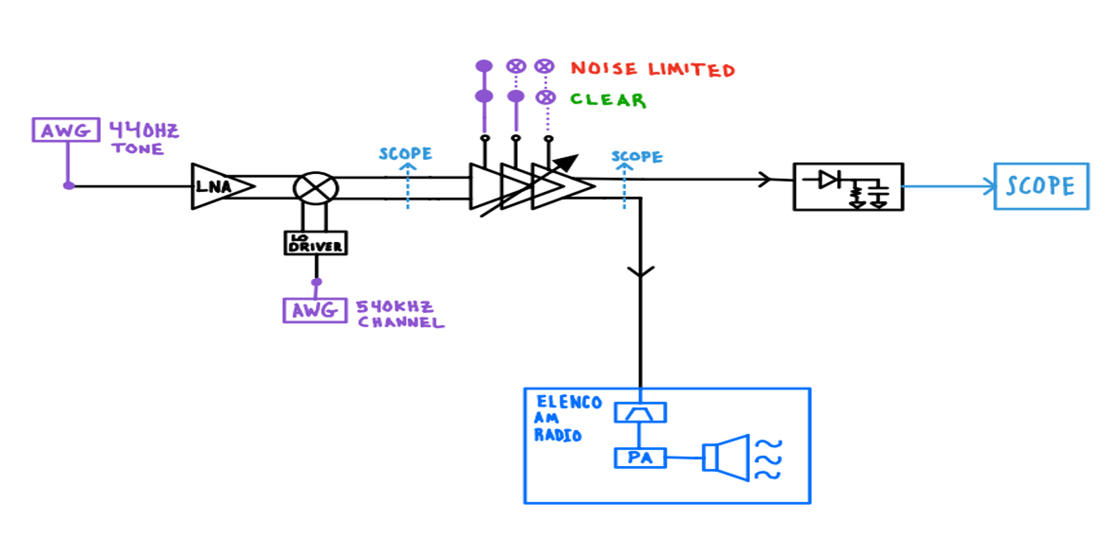
As can be seen in the video, the test was a success. The audio output of the ELENCO AM RADIO was tested for an IFA gain setting of 10x, and 100x, as well as when it is tuned to the desired channel (540kHz) and tuned away from the desired channel. The results of this test, when tuned to the LO channel, produced an audio signal limited by noise at a gain setting of 10x, but a clear 440Hz tone at a gain setting of 100x. At a gain setting of 100x, tuning away from the channel causes the audible tone to dissapear, and tuning back restores the audible 440Hz tone. These results succeed in verifying the functionality of the integrated LNA, Mixer, and IFA chain, which together implement the majority of our on-chip signal reception, processing and detection functionality.
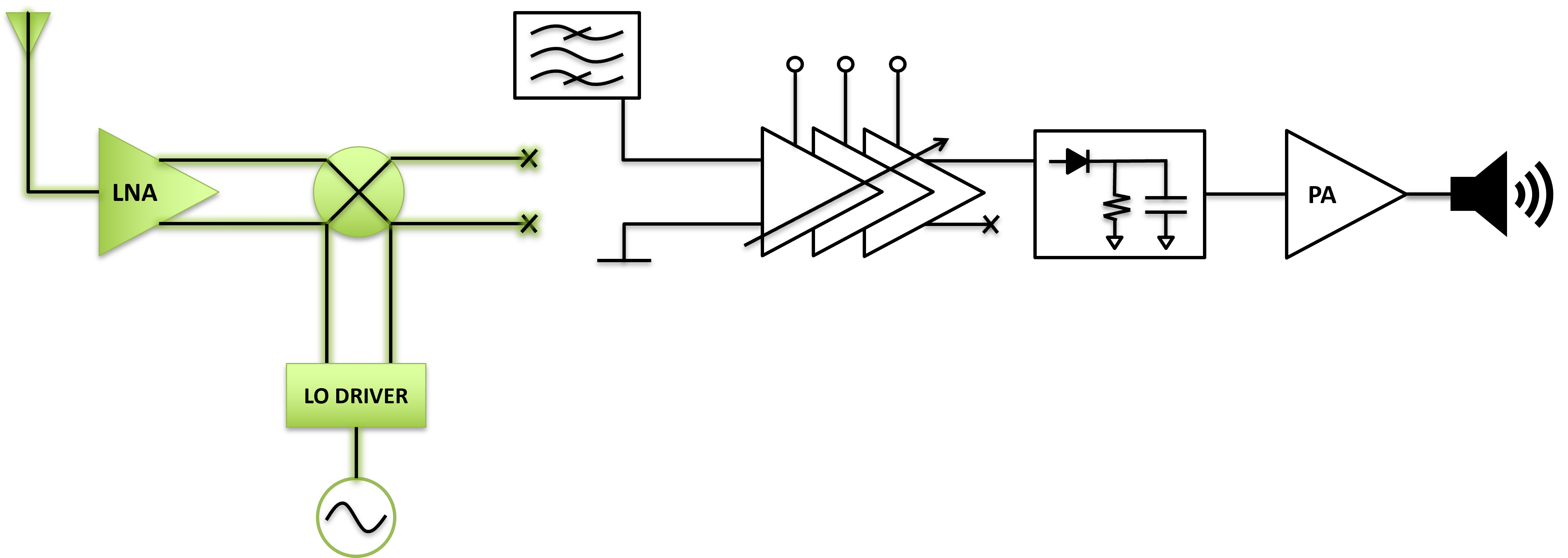
The second test result demonstrates the correct functionality of the entire RF Front-end when receiving a real AM signal off of the air, from the antenna. the LO source is provided by an AWG that outputs a square wave, which is subsequently tuned to convert the strong AM signal detected by the Antenna and LNA off of the air up to the designed intermediate-frequency (IF) of 10.7 MHz. A block diagram of the system, with the signal path and respective blocks that are succesfully verified during this test highlighted in green, is shown below.
The test results shown on the oscilliscope in the image below are taken from the two (differential) mixer outputs. The blue waveform is the input signal from the antenna. The yellow waveform is one end of the differential mixer output, the green waveform, which is completely hidden behind the yellow, is the other end of the differential mixer output. The pink waveform is a math function displaying the differential mixer output. The white plot is the FFT of the mixer output.
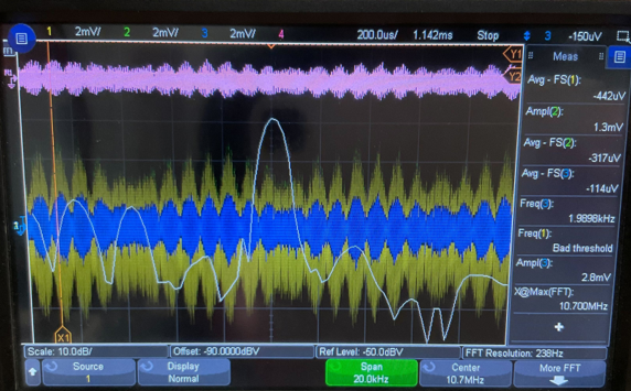
On the right side of the scope you can see waveform measurements: The input signal from the antenna has a 2.8mV amplitude (high-end of expected input signal level), and a 2kHz frequency, characteristic of the AM audio signal bandwidth (formally 3kHz). The white plot shows the FFT of the mixer output, with a strong channel (maximum FFT magnitude) centered at the desired 10.7MHz IF frequency, and with sidebands shaped as expected for an AM Radio broadcast channel transmitting audio information. The amplitude measurement of the mixer output is incorrect and can be disregarded (due to poor relative triggering and measurement resolution window) -- the waveforms clearly show the mixer outputs (yellow and hidden green) are amplified, upconverted versions of the blue input AM RF waveform.
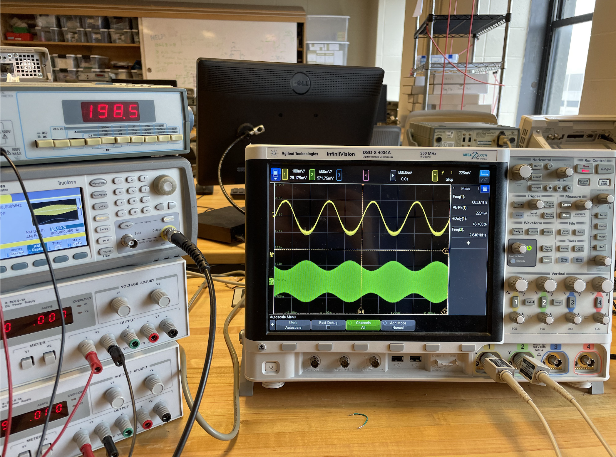
RFFE PCB Testing Results:
The initial results of the RFFE PCB testing are shown below in Fig. 4. The results are from the initial functionality tests of the RFFE blocks on the PCB. The results are promising, and show that the RFFE blocks are functioning as expected. The results show the following: The blue waveform is the input signal from an AWG. the purple and green waveforms are the differential mixer outputs. As the images move from left to right, the same scope capture is continously zoomed in on the mixer outputs. In the last capture on the right you can see the clean square waves of the mixer outputs that comprise the lower frequency sine wave. In the capture on the left, you can see that the effects of DC offset in the RFFE have been almost completely nullified; The mixer outputs show a symmetrical sine wave about a common operating point as expected. The scale of the input blue waveform is 10mV,and the scale of the mixer output waveforms is 100mV. In the middle scope capture, the blue waveform is overlayed ontop of one of the mixer outputs, showing a single ended gain of 10x, or 20dB. This yields a differential output of twice the single ended gain, or a 3dB increase in gain. This yields a differential RFFE gain of ~23dB, the simulated RFFE gain was ~25dB, the simulated and measured results are in good agreement. Further testing on the PCB is required to reliably quantify the RFFE gain, as well as other performance metrics such as noise figure, and linearity.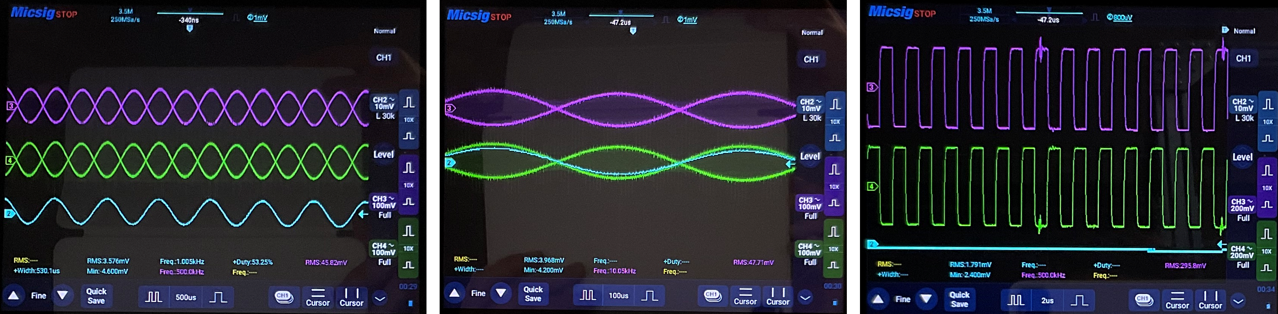
Envelope Detector and VCO Measurement Results
Detector measurement result:
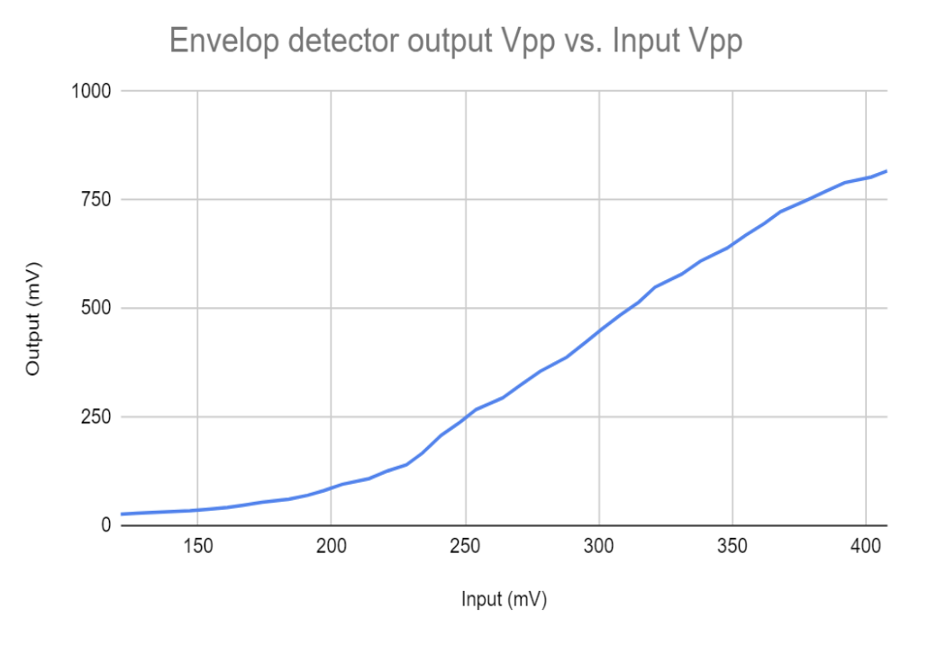
This tap-out test used a carrier frequency of 10.7 MHz. The linear part can be found between input peak-to-peak voltage from 230 mV to 390 mV. In this test, the capacitors and resistors pairs were chosen to achieve 10.7 MHz carrier frequency with message frequency from 100 Hz to 4 kHz. Moreover, since these capacitors and resistor pairs are off-chip, we can adjust those values to achieve detection at lower carrier frequencies.
VCO measurement result:
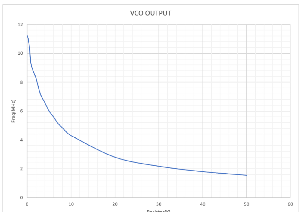
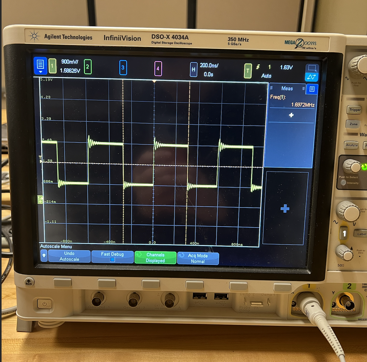
The range is from 1.8 MHz to 12.5 MHz, and the output frequency increases by 0.01 MHz for every 20 ohms of resistance adjustment.
Biasing measurement result:
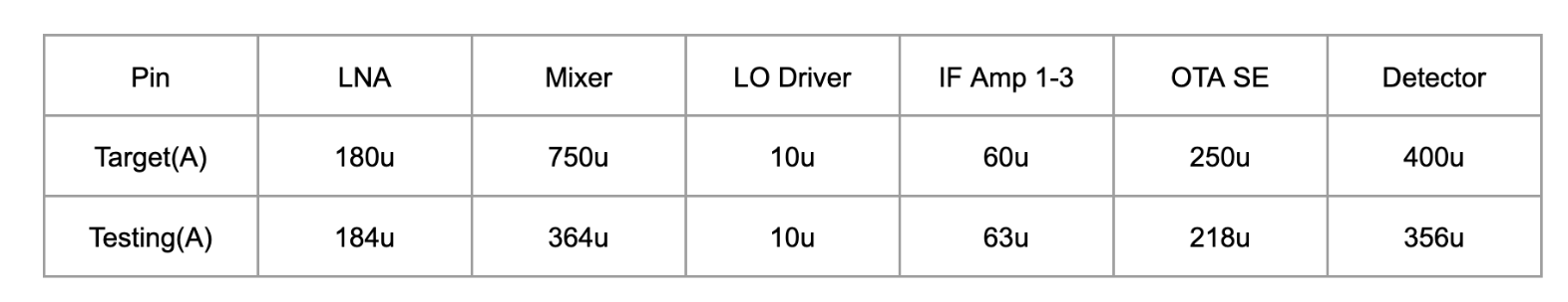
The table above displays the conclusive testing results for the biasing currents. During actual testing, there was an observed increase in the error rate for larger target currents. Despite this challenge, we proceeded to employ these biasing currents to supply power to the majority of on-chip blocks in the demonstration.