Simulation results
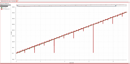
The best way to test all the possible samples to the input of ADC is to provide a slow ramp input from 0 to 1V with steps of 1 code, which is equal to 1/256. About 20 points per code were provided as input to ADC, which overall meant 20*256 codes = 5120 samples. The output of the ADC was fed into ideal DAC (programmed from Verilog-A), which was expected to come as the quantized version of the ramp input signal.
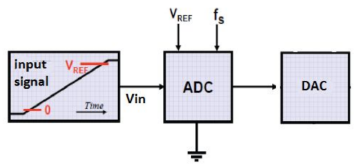
The system level static performance was observed as below:
Sample and Hold Simulations
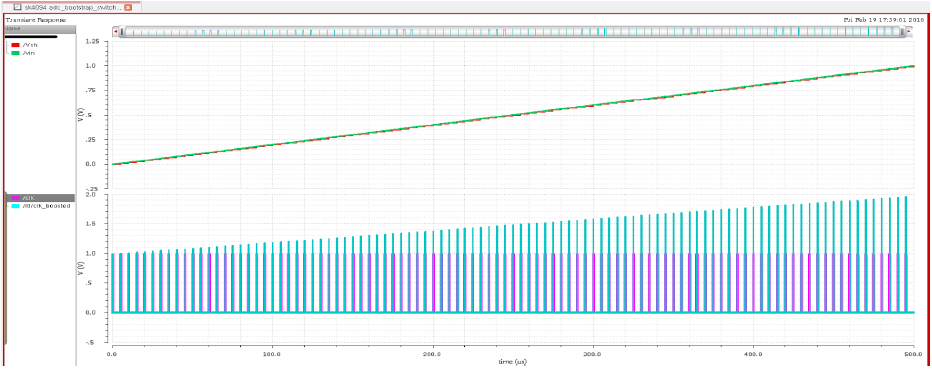
To the sampler, a continuous ramp input was given with test clock frequency of 200 KHz, duty cycle of 10% and input from 0 to 1V. Sampled voltage followed the input in track phase and the boosted clock = Vdd + Vin was also observed.
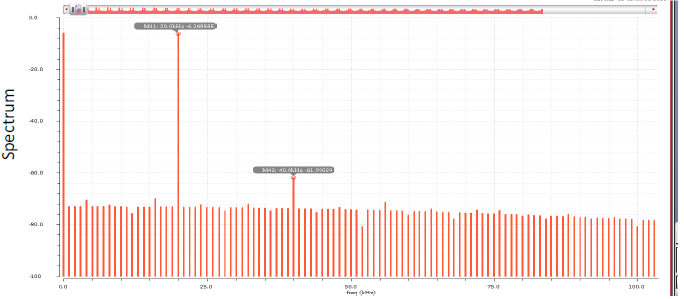
To calculate the sampling error, Beat Frequency Test was used. Hence, an input of frequency 180KHz (Fclk - Fsignal) is applied. It was observed that the maximum spur occurred at the second harmonic (40KHz). For accurate DFT computation, Tsimulation = 1/(Fres = 1KHz) = 1ms was calculated. Number of points used in DFT simulation window were 2^14. Thus, to obtain sufficient transient points, calculated Tstrobe = 1ms/(2^14).
The charge injection is reduced by using small main switch and a large hold capacitance. Using tt, ss, sf and fs process, simulations, it was observed SFDR varied from 48 dB to 61 dB. For the Bootstrapped switch circuit, sampling error was found to be 1.1 - 1.5uV for Vin = 0-1V.
DAC Simulations
DAC simulation was different in a way, that it was first modelled in MATLAB along with the SAR Logic. The 5120 -sampled output of S/H circuit was taken and fed to the SAR-DAC model. It was experimented with ideal scenario first and then with inclusion of factors like comparator offset and dac_noise (KT/min_cap). Based on the output of the DAC, quantization error was calculated. RMS of the quantization error gave the noise power, from which minimum DAC unit capacitance was calculated and then tried on layout. The simulation results of the Cadence layout were taken and the mean and standard deviation of DAC output values corresponding to each set of 256 codes were in fed in the MATLAB code. Using the data, DNL and INL errors were calculated to check the linearity, and both came out to be less than 0.25*LSB.
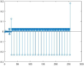
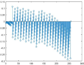
It was observed non-ideality of DAC output was causing the gain-error not the linearity error.
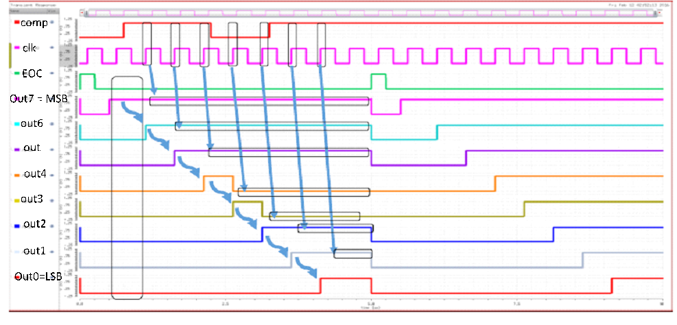
SAR Simulations
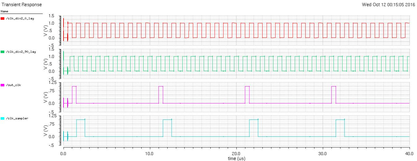
SAR, being one of the digital blocks, had an easier simulation method. The major area in SAR logic is covered by repeated rectangular blocks which represent D-flip flop (used as register). The inputs to the SAR block are comparator output ("comp" signal) and the clock. The EOC signal acts on clk_90, which marks the beginning on binary search algorithm. It takes 10 cycles to produce one digital output from the given input sample. Thus, sampling clock is always 10 times less than SAR clock.
Comparator Simulations
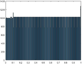
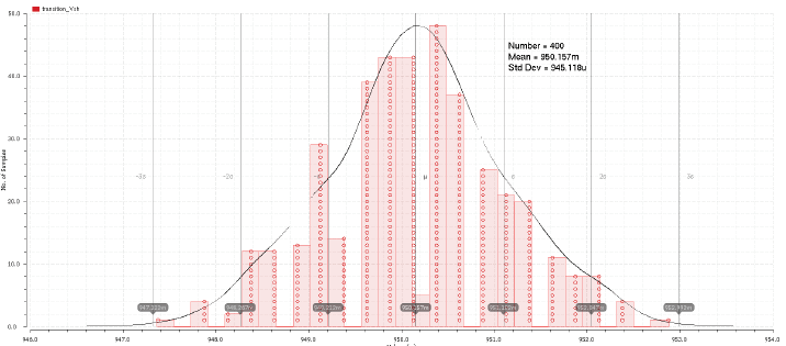
The main challenge was to find the sensitivity and error variation in the comparator. To get this, a histogram of number of samples per offset voltage was created. Sensitivity of the comparator was found to be 0.1 mV and common mode offset voltage's worst value was 0.5mV. Input capacitance varied from 123fF to 460fF when common mode input voltage varied from 0-1 V respectively.
Timing Simulations
The timing block being the other digital circuit is used to create 200KHz, 2MHz and 2MHz-90-degree phase shift clocks.