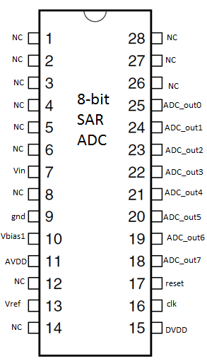
Pin Diagram
The MOSIS fabricated chip had the following pin diagram:
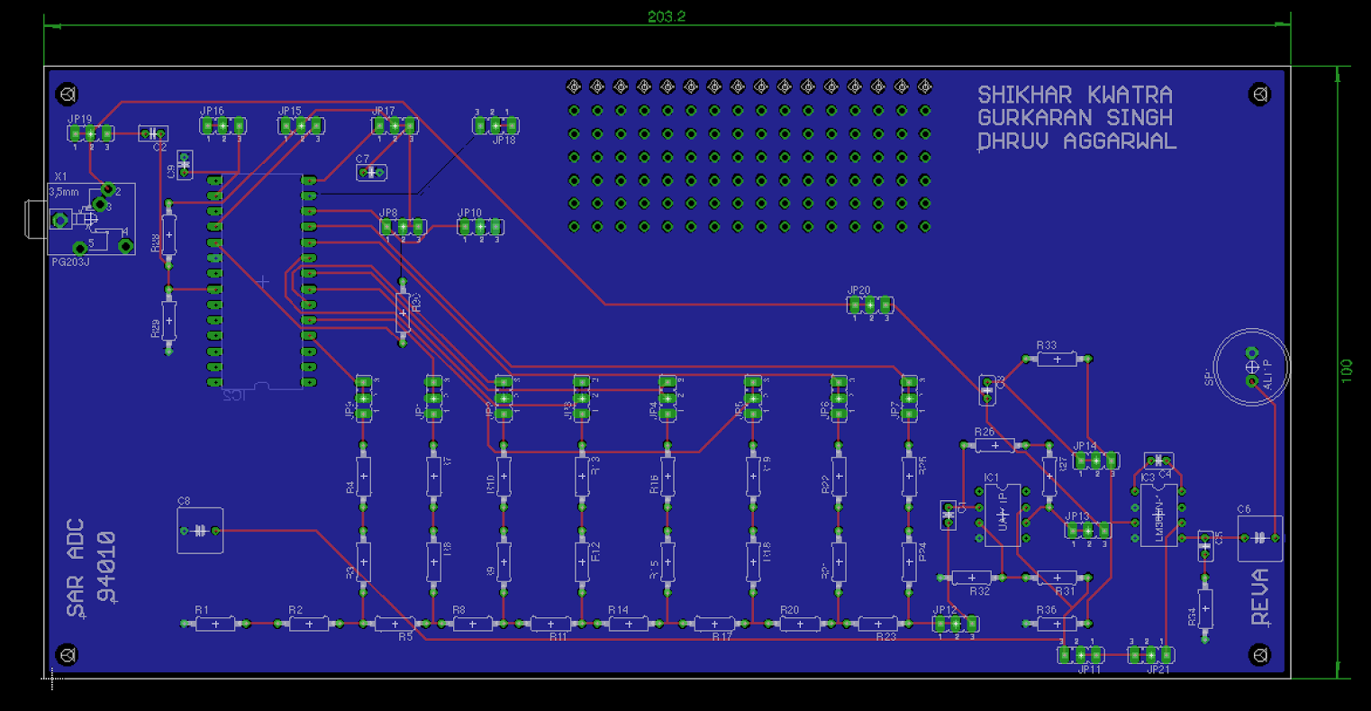
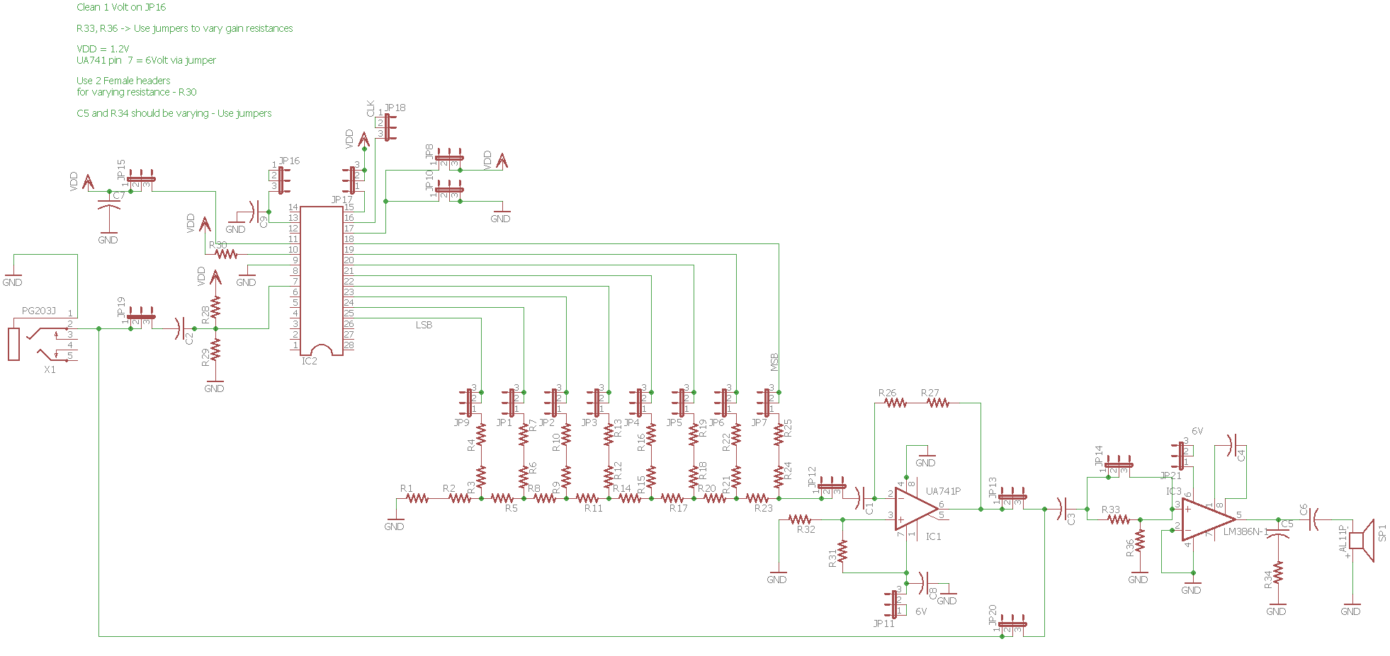
PCB Design
To design the peripheral components with the fabricated ADC chip, a custom PCB is required. Two-layer board design was sufficient for testing the performance of the ADC chip inculcated with the peripheral circuitry. To keep the PCB board organized and provide ease in debugging for enhanced observability and testability, jumper pins were connected at all the inputs and output pins of the 8-bit SAR ADC in conjunction with R-2R ladder based DAC circuit and audio amplifier. 1 Meg resistors are used for R-2R DAC circuit which have a precision of +/-5%.During the process, we use Eagle software for PCB design and PCB Minions as our PCB manufacturer.