Introduction
The goal of this project was to design and tape-out a low power 8-bit Successive Approximation Register Analog-to-Digital Converter (SAR ADC) and report the measured performance of chip.
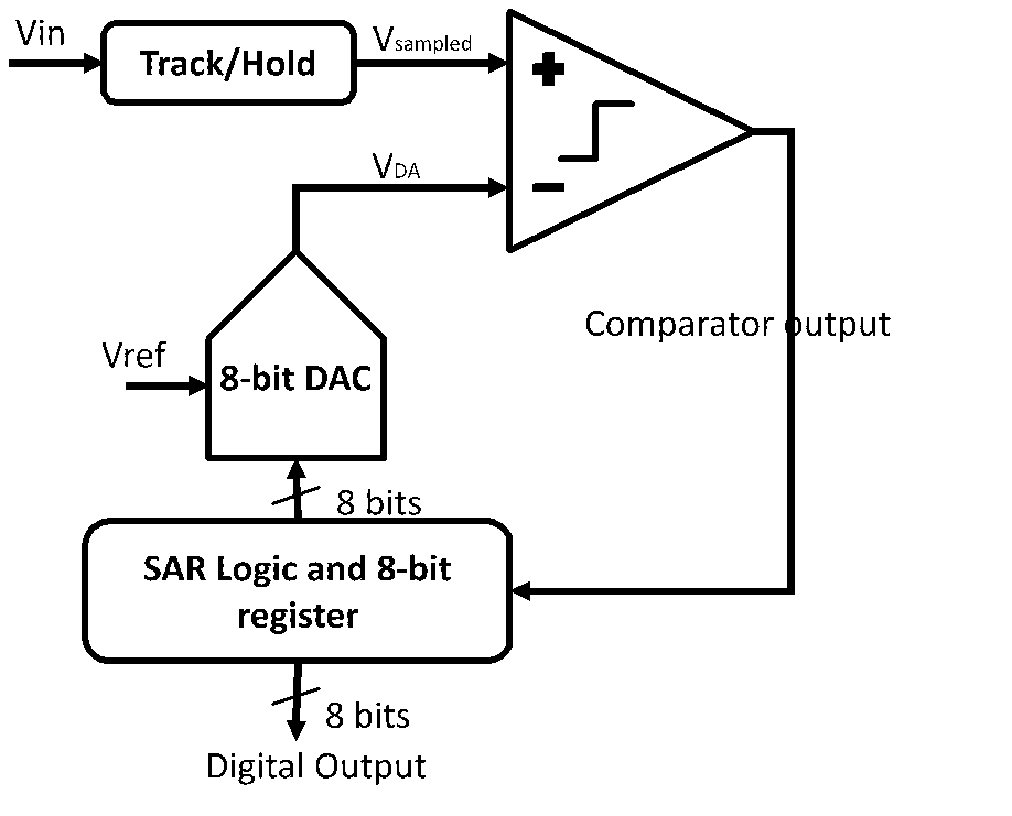
The ADC was designed within 1 mm2 area and operates on 1V Supply voltage. The chip was then demonstrated using audio input from the laptop, passing that through ADC, reconstructing through R-2R ladder DAC and then playing it through the speaker via Audio amplifier. The block diagram of the ADC is described in figure 1. The chip consists of 4 major blocks - Track and hold, comparator, SAR Logic and DAC. The input analog signal is sampled by S/H circuit, which is then sent to comparator. Based on the comparator output SAR logic decides whether the next bit is 0 or 1, and produces 8 bits. These 8-bits are again converted to discrete signal using DAC to serve as the reference for the Comparator to decide if the next bit will be 0 or 1. It takes 10 cycles to produce one full output.
The power consumed by the ADC has been found to be 3.36uW. The value of SNDR is observed as 41.20 dB. Effective Number of bits (ENOB) is computed as 6.55. The maximum value of INL and DNL is 1.400 LSB and 2.600 LSB respectively. Detailed measured results of the core ADC chip is described in System Level Specifications.