Transistor Level Design
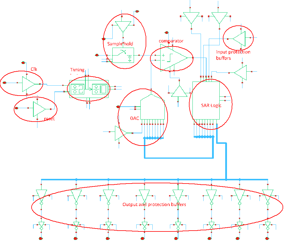
The ADC consists of 5 major blocks - Sample/ Hold block, comparator, SAR Logic block, 8-bit DAC and the timing block. Each block is explained below.
Sample/Hold Circuit
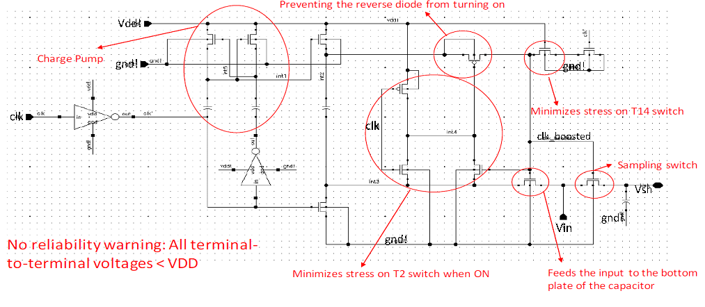
The S/H circuit captures the input analog signal based on a sampling frequency. In the project, the sampling frequency is 200 KHz. The bootstrapped switch circuit is described in [1]. The advantage of using such configuration is that it improves the linearity of switch for the entire input voltage range.
In the basic Bootstrapping, inserting a battery can keep the device in constant Vgs mode, which preserves linearity, even with the large input voltage. The battery is approximated by a pre-charged capacitor and several MOSFETs acting as switches as given in the schematic. In the sampling mode, the capacitor keeps the device on. In the hold mode, the MOS is to be turned off and the capacitor must be recharged to Vdd.
Thus,the following bootstrapped schematic was used.
Charge-Redistribution Digital-to-Analog Converter (DAC)
The SAR ADC has an internal DAC, which at every clock converts the 8-bit SAR Logic output into discrete signal, which is fed into the comparator. This feedback is used to decide the next bit of the SAR output. In the project, a Charge redistribution DAC with binary weighted capacitance [3] configuration is used. Each switch capacitance pair represents a bit of the 8-bit input.
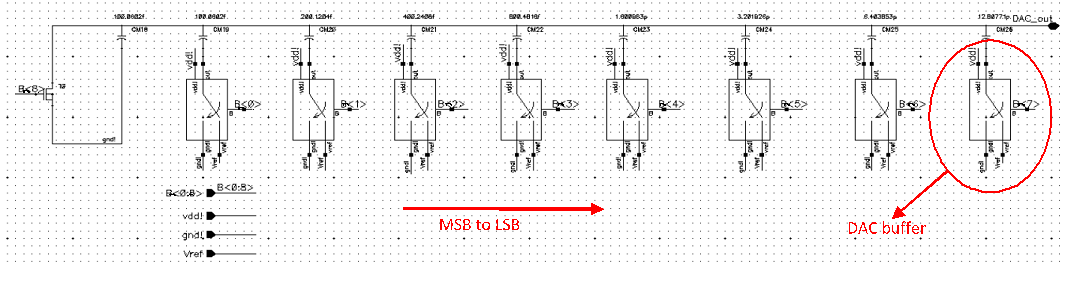
The minimum value of capacitance (in DAC order C,2C,4C,...,128C) is chosen by:
C = H*(K*T/noise_power)
where
K = 1.38064852e-23
T = 298
H = sum((0.5)^p) where p = 0:1:7 (for 8 bit DAC)
Theoretically, the noise power should be comparable to quantization noise power which is (delta^2)/12, where delta = Vref/2^N. N is 8 in this case. This gives minimum capacitance C = 6fF in theory. However, in the project, MIMCaps are used whose minimum capacitance is 100fF. Inverter sizes in DAC switches were adjusted to achieve T=RC which should be much less than clock period. Parasitic capacitance at the DAC output was approximated to 150fF, determined from SP analysis.
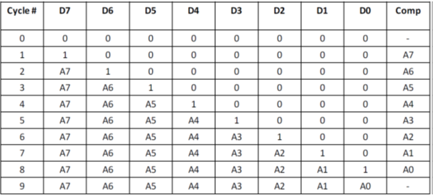
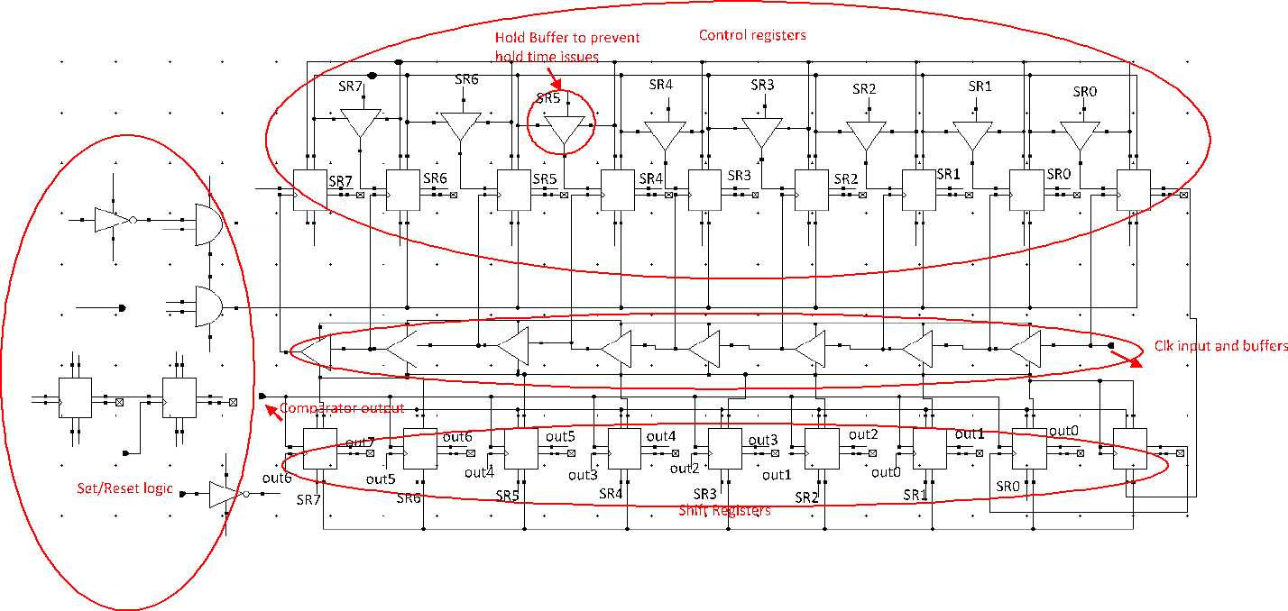
Successive Approximation Register (SAR Logic)
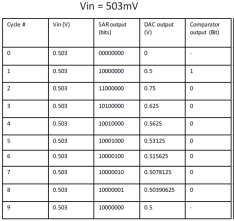
The SAR operation is based on binary search algorithm. A SAR logic takes 10 cycles (8bits + 2 extra cycles) to generate one output. Hence, if the sampling rate is 200KHz, 2MHz of clock is required for SAR. In this logic, the bits are represented by the registers D7-D0. In the first cycle, all the registers are set to 0. Then in cycle#1, MSB (D7) is set to 1. This results in binary code '10000000'. This is converted to discrete output using the DAC and compared to the sampler output. If the result of the DAC output subtracted from the sampler output is less than 0, then the MSB is set to 0. In cycle#2, next MSB (D6) is acted upon in the same way. Thus, this goes on till all the bits are converted.
Note that the quantized output will always be less than the input voltage, within 1 LSB limit in theory. An example for Vin = 503mV is given below.
The SAR Logic schematic consists of 2N flops (N=8): They are the 8 shift registers and 8 control registers. The Comparator output acts as the control bus logic for computing the output.
As described in [4], the SAR schematic has a set/reset logic as follows:
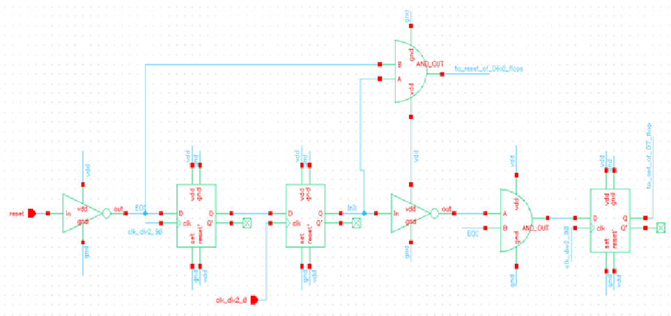
This logic is used to reset the flops at the start of conversion cycle as well as indicate EOC (End-of-Conversion) signal to the logic. To create output well within the cycle time, both clock and clock_90 (90 degree phase shifted clock) are used. When reset is raised, EOC goes low and it resets all the flops. When reset is low, EOC goes high, feeds in 'init' which keeps resets in all flops high (thus, inputs of flops are maintained). The combination of init and EOC signal then feeds into the set of D7 (MSB flop) and hence, the conversion cycle begins. The schematic describes the overall picture of SAR logic:
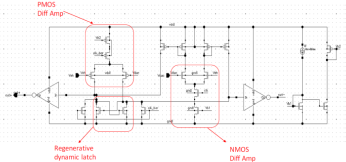
Comparator
The comparator is used to take S/H output and DAC output, find the difference and send it to the SAR logic. Both nMOS and pMOS differential inputs are used to capture rail to rail 1V input swing. Clock switches are connected at drain mode since they introduce less voltage offset.
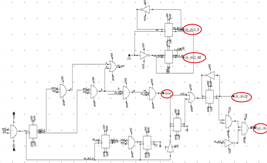
Timing Logic
Timing logic is used to produce different clocks required in different places in the ADC. The input of 4MHz is given, which is first sent to divide by 2 counter. This produces 2MHz clock required for the SAR and DAC circuit. Then this clock is sent to divide by 10 counter which produces 200KHz clock required for sample and hold operations. Also, the 2MHz clock is also passed into 90-degree phase shifter to produce clk_90.