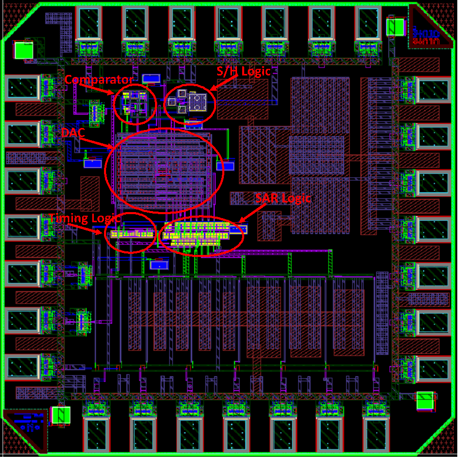
Layouts
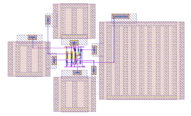
1. S/H Layout
Layout area of S/H circuit is mostly dominated by the MIMCaps used for charge pump, Bootstrapping and load.
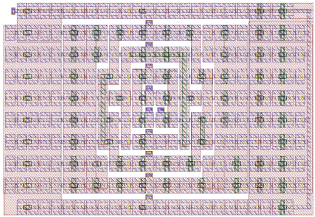
2. DAC Layout
The major challenge in the DAC is the choice of capacitor array layout as well as their placement. The concept of capacitor array layout is explained in [5]. In the project the capacitors are laid out in a grid network, where there is a need to create all values of capacitors, beginning from C (unit capacitance), then 2*C, 4*C, 8*C, 16*C, 32*C, 64*C and finally 128*C. Implementation of larger capacitance can be done by connecting unit capacitance cells in parallel. Here, the capacitors are laid out in common centroid matching arrangement.
The numbers in the figure shouwn below indicate the capacitance value to which the cell belongs.
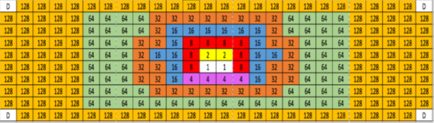
The advantage of this layout is that no cross connections are required, that is, all capacitors belonging to same group can be connected either horizontally or vertically. For a perfectly balanced layout, the centroid mismatch should be at (0,0). Column wise, the layout is perfectly symmetric, so the column centroid mismatch is 0 with centroid at 13.5. Row wise, the layout is not symmetric. By looking at all the combinations produced by moving around capacitances with value 64,32,16,8,4,2 and 1, it was found the centroid varies between 4.5 to 7, hence, the maximum mismatch in row is 2.5. If the width of one cap cell of value 60fF is 5.24 um, then total mismatch is 2.5 * 5.24 ~ 13 um.
Total area analysis: 26 col * 10 rows.
1 cap dimension = 5.24 * 6 sq. um
Total area = 26*5.24 * 10 * 6 = 156 um * 60 um.
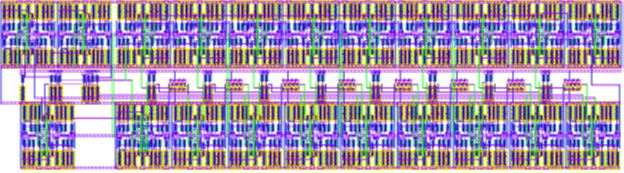
3. SAR Layout
The major area in SAR logic layout is covered by repeated rectangular blocks which represent D-flip flop (used as register).
4. Comparator
The differential amplifier transistors in the comparator are to be placed very symmetrically in order to minimize the mismatch. Hence, common centroid topology is followed.
5. Timing Logic
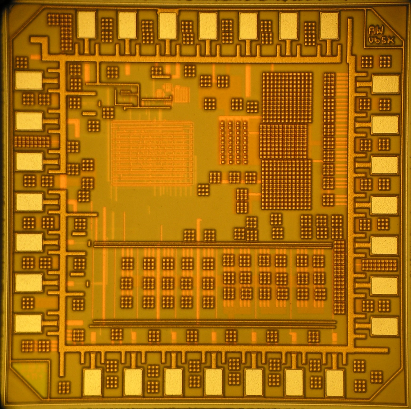
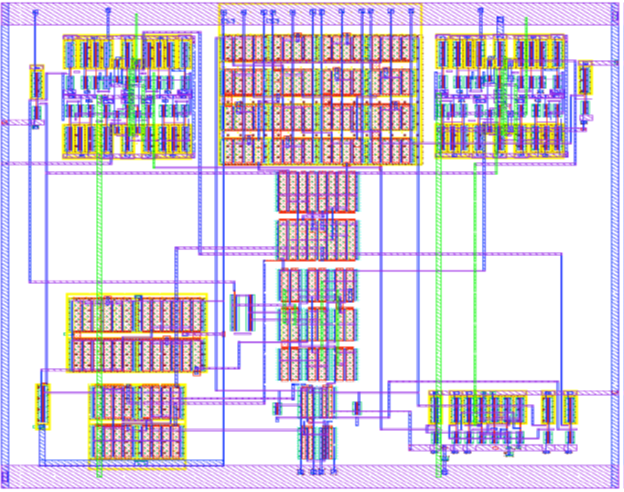
6. Top Level Layout with Chip Edge
After all the individual blocks are created and tested with DRC and LVS clean, next big thing becomes assembly and placement. Analog blocks like sample/hold circuit and the comparator were placed near the chip edges to minimize signal loss of the sensitive input signals. ESD protection was provided to inputs of the top-level circuit. Bond pads were created and the circuit was placed. Since, the circuit is low frequency, liberty was taken to create long wires from SAR logic to the ADC outputs. Later, metal filling was done to prevent metal density issues given by DRC.