
System Design
The project is partitioned into two parts. The IC-chip handles all the digital logic computation, and PCB supports the I/O interfacing and peripherals.
IC Design
The top-level block diagram of the IC chip is shown below. It consists of a series of frequency dividors (modulo counters), one multiplex driver, and a display decoder.
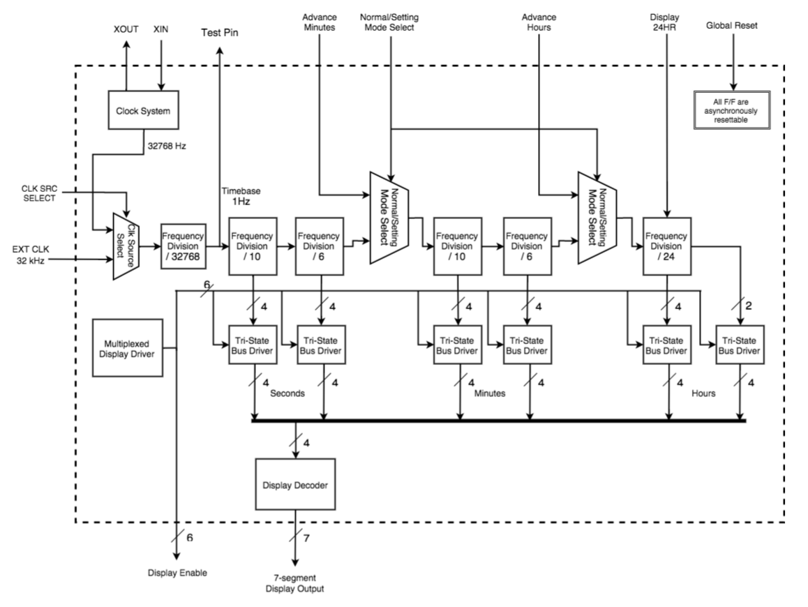
Apart from the user inputs and pins for settings, the IC chip takes an oscillation input from a crystal that resonants at 32,768 Hz. The oscillation is down-converted to 1 Hz through a frequency dividor with a factor of 32,768. It feeds to the ones-digit of the second count, which feeds to the tens-digit of the second count, so on and so forth. For all ones-digits, the frequency dividor is essentially a modulo-10 counter with overflow output toggling to the corresponding next-stage tens-digit frequency dividor. The tens-digit uses a similar module-6 counter. Each digit's value is also output to a common bus in the format of BCD, binary coded decimal. The multiplexed driver grants the ownership of the common bus with a Round-robin scheduling, i.e. each digit owns one-sixth of the refresh cycle.
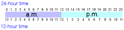
Our digital clock supports time display in two forms, 12-hour display and 24-hour display. Conversion between 12-hour display and 24-hour display follows the chart below.
With the counting sequence defined for each digit, we designed the finite state machines (FSMs) for different functional blocks. All of these FSMs are designed in a Moore Machine style such that the outputs of the FSM depend only on the current state, but not on the inputs. Since all of our FSM designs follow the same strategy, we will focus on the modulo-24 counter for the purpose of demonstration.
We need at least 24 states for outputing 24 different modulo-24 integral values in the range of [0, 23]. We need at minimum 5 bits of storage elements to store the state variable. The state machine starts counting from 0, and at each clock cycle, it counts up by 1. Therefore we have a deterministic relationship between current state and the next state: when the current state is 0, the next state is 1; when the current state is 1, the next state is 2; so on and so forth until when the current state is 23, the next state is 0. Declare the current state variable to be a 5-bit variable ps4 ps3 ps2 ps1 ps0, and the next state variable to be a 5-bit variable ns4 ns3 ns2 ns1 ns0, then we have the truth table between current state and next state. Either by solveing the corresponding Karnaugh map or by running some CAD software, we have the Boolean functions for the next state variable represented using current state variable. With these Boolean functions, we can design the combinational circuits for the next-state logic for the FSM. Similarly, we have the Boolean expression for the primary outputs in terms of the current state variable, thus we have the output logic for the FSM.
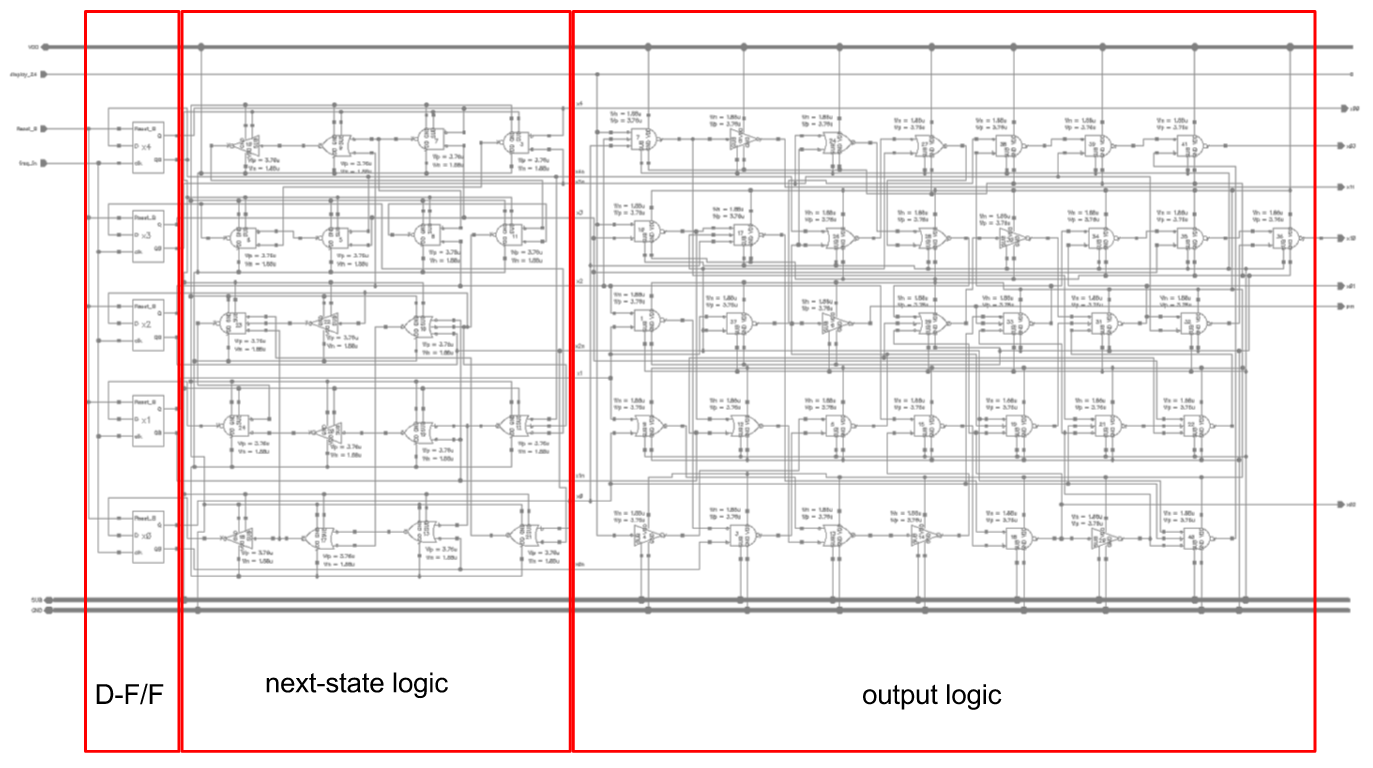
The other FSM designs are extremely similar. To view the layouts of these FSM implementations, please visit the IC layout page from the navigation bar above.
Among the design process, we tried some very useful softwares to derive logic expressions based on a given Boolean Truth Table. For example, we used espresso and Logic Friday. Espresso uses a text-console based interface and it is available for most UNIX OS, while Logic Friday is a free software that has a user-friendly graphic-user interface.
Interfaces
To display a digit on a 7-segment LED display, it requires a minimum of 8 control pins (7 control inputs for the segments and 1 for the common anode). To display 6 digits in parallel requires 56 control signals. This number exceeds the number of pins provided by a DIP28 IC packages. Hence, we used the method to time-multiplex some control signals, which reduced the number of control pins down to 14.
The drawback of time-multiplexing signals is that it introduces some performance issue related to the LED displays. Since the multiplexed enable signals cannot align perfectly and LEDs are not shut off instantly after the enable signal gets deasserted, we see a dim shadow of the previous digit in each digit. This could be resolved on the PCB level, but may involve a much complicated LED driver circuit.