
PCB Design
It is part of our design to create a compatible PCB to support the Digital Clock IC-chip. We want to build a working project; moreover, we want to make it look good.
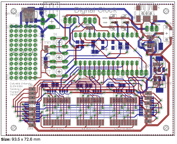
PCB overview
The PCB has a full support to run the Digital Clock IC-chip. It has a power supply circuit, digital IC pin connection circuits, LED driver circuits, and an oscillator circuit. Once IC-chip is plugged in, the PCB itself is a stand-alone device.
We design the PCB in Eagle CAD software. The dimension of the board is 9.35 x 7.26 cm, about the size of a wallet that fits in your jean pocket.
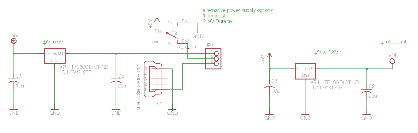
Power circuit
We designed the PCB to run on multiple power supplies. It can be powered either by a portable 9V Dura-cell battery through the power jack connector, or by a 5V stationary wall-plug charger through the mini-USB connector. In either case, the board provides 5V and 1.8V for the rest of the IC-chip.
Selection of the power sources is done by the shunt connection next to the ON/OFF switch on the board.
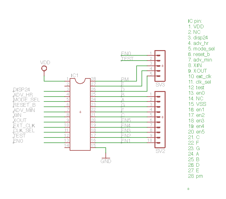
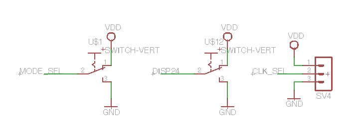
IC pin connection
The heart and brain of this project is the Digital Clock IC-chip. The board provides peripheral supports, like I/O interfacing. The IC-chips that MOSIS manufactured come with the DIP-28 packages. Solely for the testing purposes, we extended all output pins to pin headers on the board.
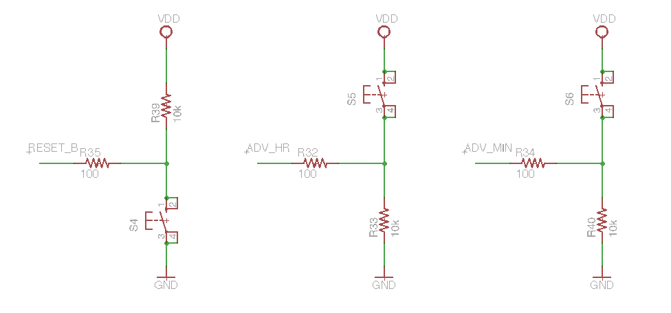
User inputs (reset, +hour, +minute) are designed in the push-button style; while setting inputs (mode select, 24/12 hour display, clock select), which are set only once at the beginning, are designed using either slide switch or shunt connector.
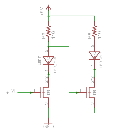
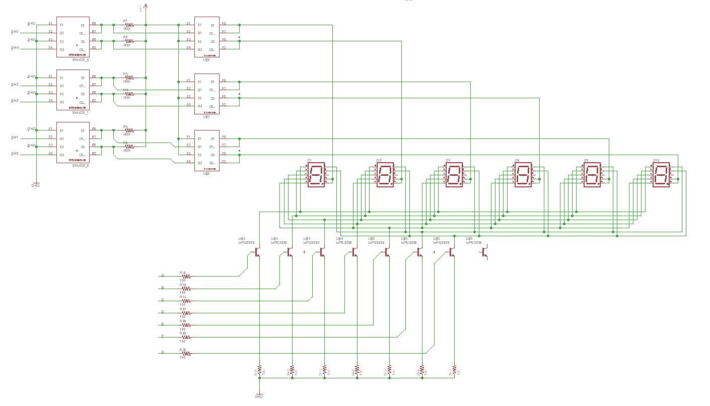
LED driver
There are two parts of LED driver circuit, one for the AM/PM indicator and one for 7-segment multiplexed time display.
The two LEDs of the AM/PM indicator are controlled by a single digital output pin, PM. That digital output pin drives the NMOS to control the on-off switch of the PM LED. The AM LED is controlled by another pull-down NMOS.
The 7-segment LEDs require a much sophisticated driver circuit. There are 6 enable signals controlling the on-off of the 6 digits, and there are 7 control signals controlling the on-off state of the 7 segments of the enabled digit. The enable signals, through the level shifters made of PMOS and NMOS, are connected to the common annode of each digit, while each segment of a digit are connected to a common LED driver circuit using BJTs.
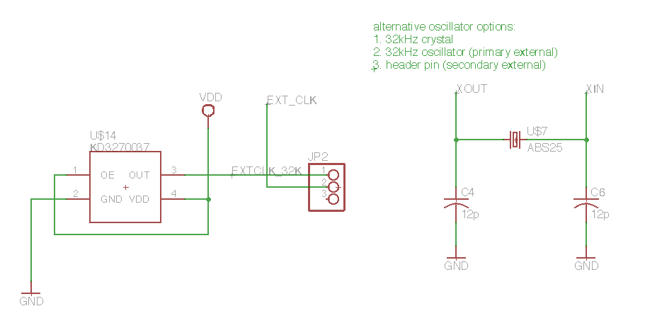
Oscillator circuit
Because of the skeptical nature of engineers, we designed oscillator circuit with multiple osciallting sources. The primary source is an on-board 32.768kHz crystal, with the oscillator circuit integrated inside the IC-chip. The secondary source is an on-board 32.768 oscillator IC. The selection of the oscillators is done by shunt connector.
Metallic logo
We created a metallic logo layer using the logo of Columbia Engineering. The logo is at the topper copper layer and we added a square solder mask on top of that to reveal the image.
PCB Product
We sent the PCB design to Advanced Circuit for fabrication. In order to generate the Gerber files that are acceptable to the Advanced Circuit standards, we created the CAM process job for each layer independently. To view the 3D model of the PCB, we used the online tool called webGerber.
