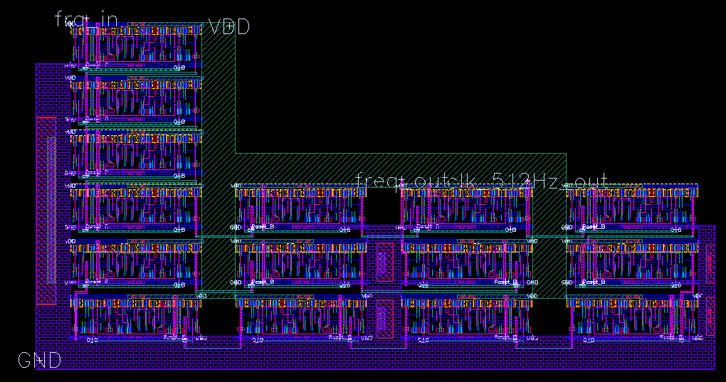
IC Layout
IC design and simulation was done using the Cadence Virtuoso CAD software, licensed to Columbia University Circuit and Embedded System Lab.
Basic Cells
For any digital circuit, we need a set of basic logic gates to implement its digital logic functions. These digital logic gates form a finite basis of all logic expressions. Some common finite basis are {AND2, OR2, INV}, {NAND2}, etc. Although the logic gates of a finite basis guarantee the completeness of all logic functions, it might not be an ideal circuit in terms of complexity, area, and power. Hence we implemented extra gates to accomodate a better design.
We designed these digital logic gates using static logic family implementation, i.e. CMOS VLSI design style. In contrast to static logic family is the dynamic logic family, which normally implements faster logic gates using smaller area. However, the tradeoff of such design is complexity, which we avoided to guarantee a working final project.
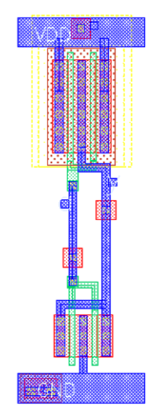
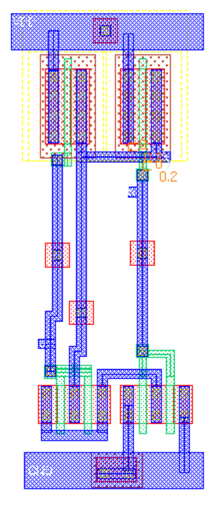
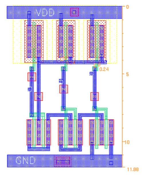
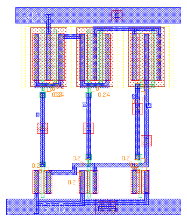
Presented below is some basic cell layouts from our design files.
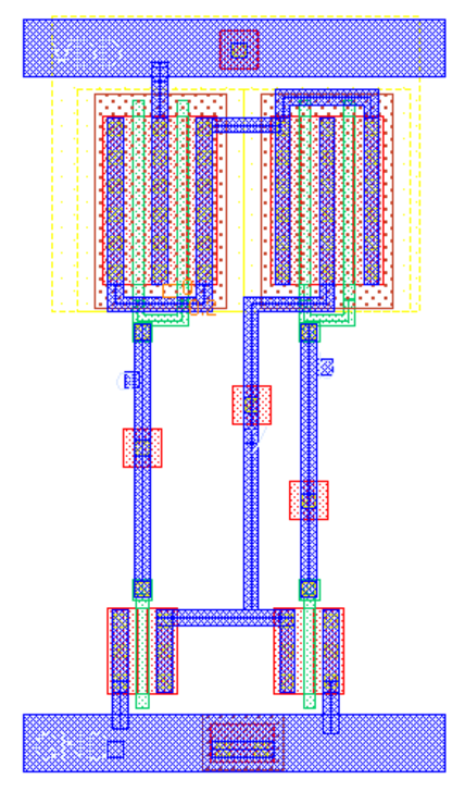
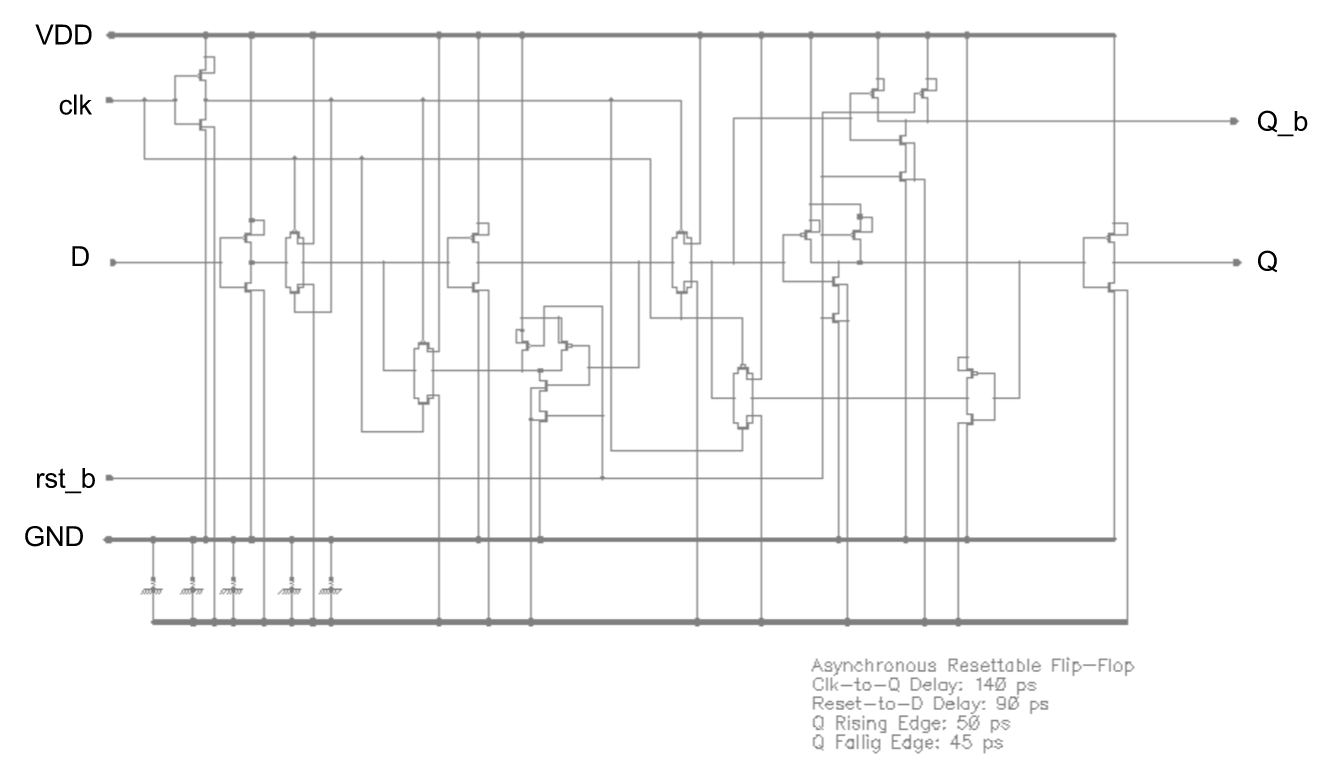
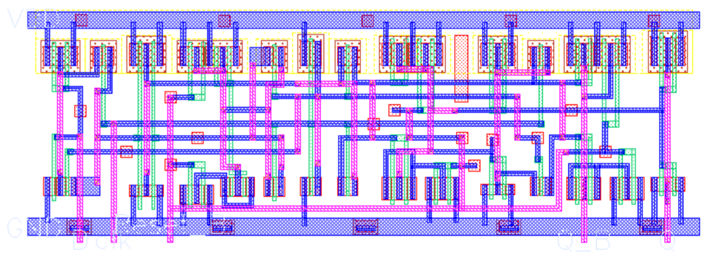
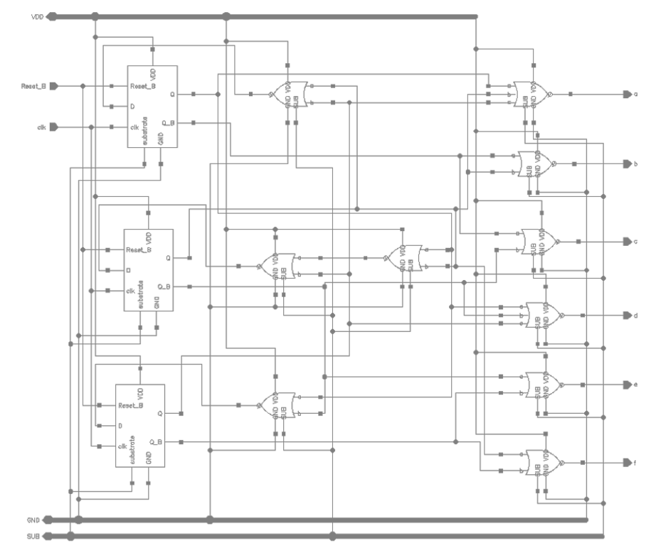
Apart from the combinational circuit elements above, a digital circuit normally requires certain storage elements. A common storage element is known as D-Q Flip-Flop, acronym DFF. We designed our own DFF with asynchronous reset. The following figures are the schematic and the layout of DFF.
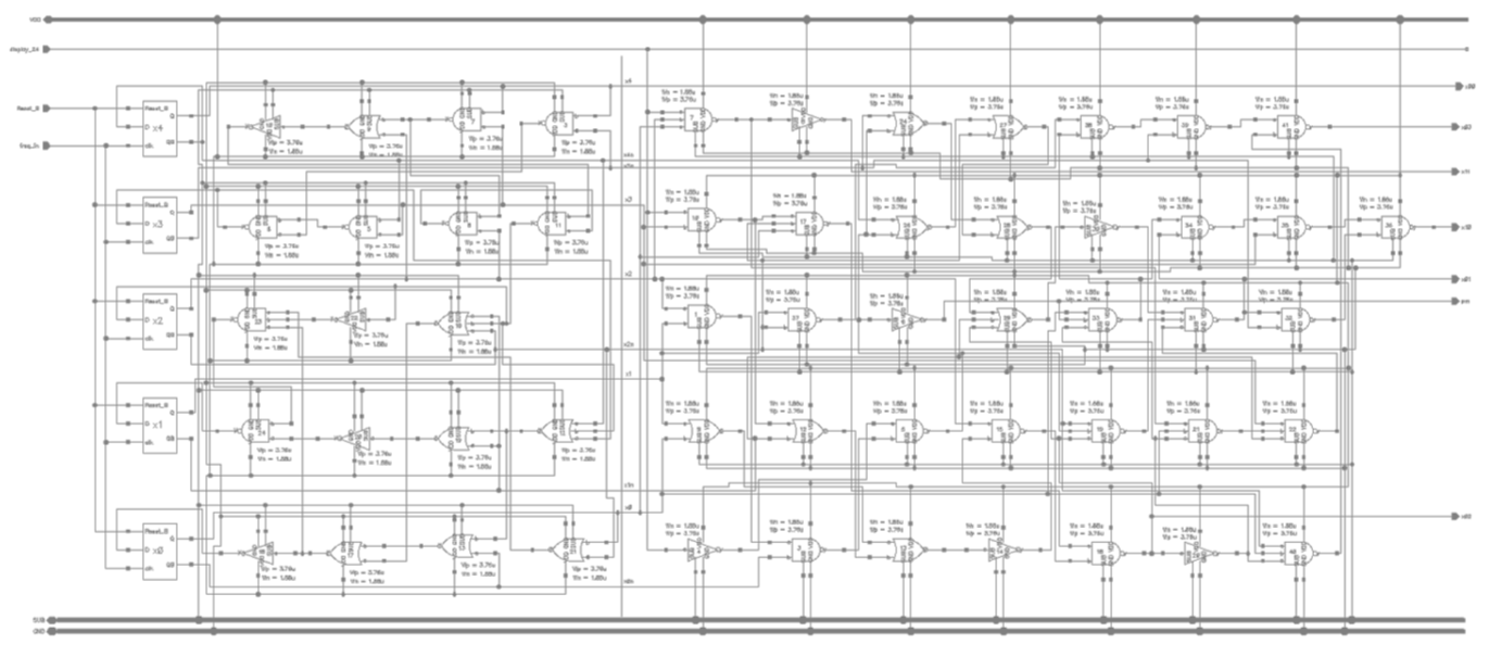
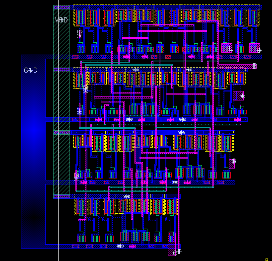
Functional Blocks
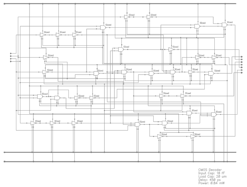
Using the basic cells above, we constructed a couple of functional blocks. For instance, we implemented a set of modulo counters, multiplex driver, converter from BCD to 7-segment outputs, and input debouncer circuit.

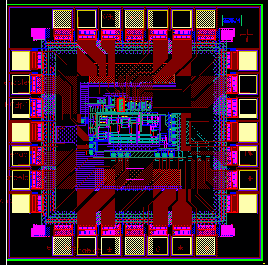
Top Level
At top level, we connected all functional blocks together and binded them to the correct input pads.