
PCB DESIGN
PCB SCHEMATIC
A 2-layer PCB was designed using KiCAD to verify the functionality of the chip within the whole system. Fig. 42 shows the schematic of the PCB board, with off-chip components including an LDO, an Arduino Uno R3, a photodetector, LEDs, level shifters, capacitors, resistors and test pins.
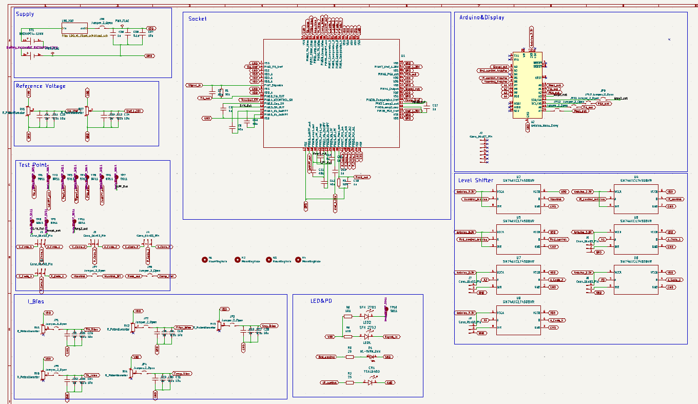
Fig 42. PCB Schematic
PCB LAYOUT
Fig. 43 shows the PCB layout in KiCAD. Components are placed to minimize distance and overlap of routing, reducing noise added by the PCB.

Fig 43. PCB Layout
LED AND PHOTODETECTOR

Fig 44. LED and Photodetector Schematic
LEVEL SHIFTERS
Level shifters are placed on the PCB to control the arduino voltage output to LEDs and digital output to control pins on the chip. This because arduino output voltage (3.3V) is higher than the voltage input of the chip (2.5V).
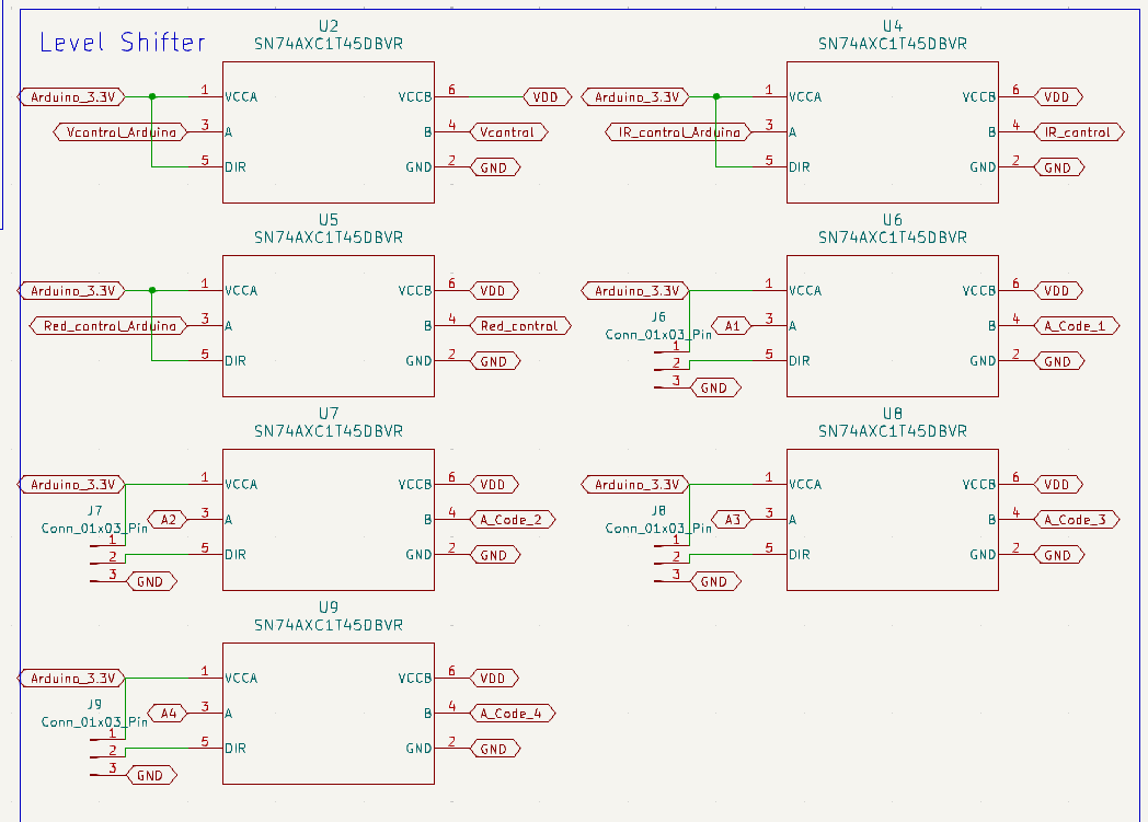
Fig 45. Level Shifter Schematic
BIAS CURRENTS
Bias currents are provided by adjusting a potentiometer, with decoupling capacitors placed to prevent sudden changes in current due to supply voltage.
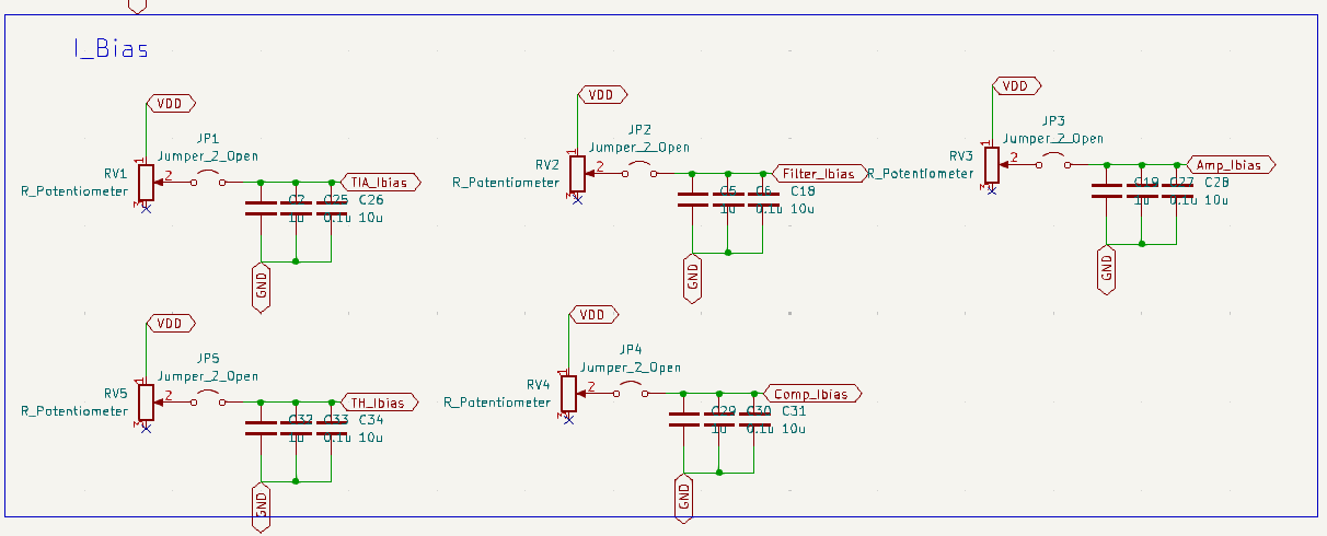
Fig 46. Bias Current Schematic
POWER MANAGEMENT
An external LDO, together with decoupling capacitors, are used to provide a stable 2.5V supply to the chip and PCB components. Voltage dividers are used to generate reference 1.25V voltage to chip and TIA. This allows us to adjust TIA reference voltage during testing.
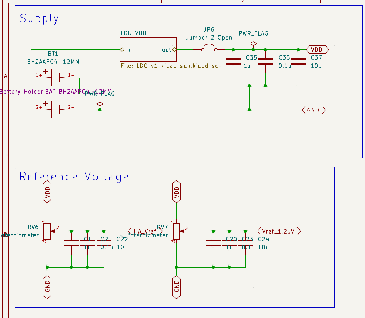
Fig 47. LDO and Reference Voltage Schematic