
CIRCUIT DESIGN
SCHEMATIC BLOCK DIAGRAM
The system block diagram is shown in Fig. 5. We utilize an automatic gain control loop with feed-forward to control the amplification of the PGA, maximizing the AC amplitude before the signal enters the comparator. This ensures higher accuracy in the comparator stage and the final output waveform.
We also utilize a track-and-hold system to reduce the power consumption of the chip. The track-and-hold allows the duty cycle of the LEDs to be set to a minimum of 10%, with the control voltage of the track-and-hold being set to same duty cycle.
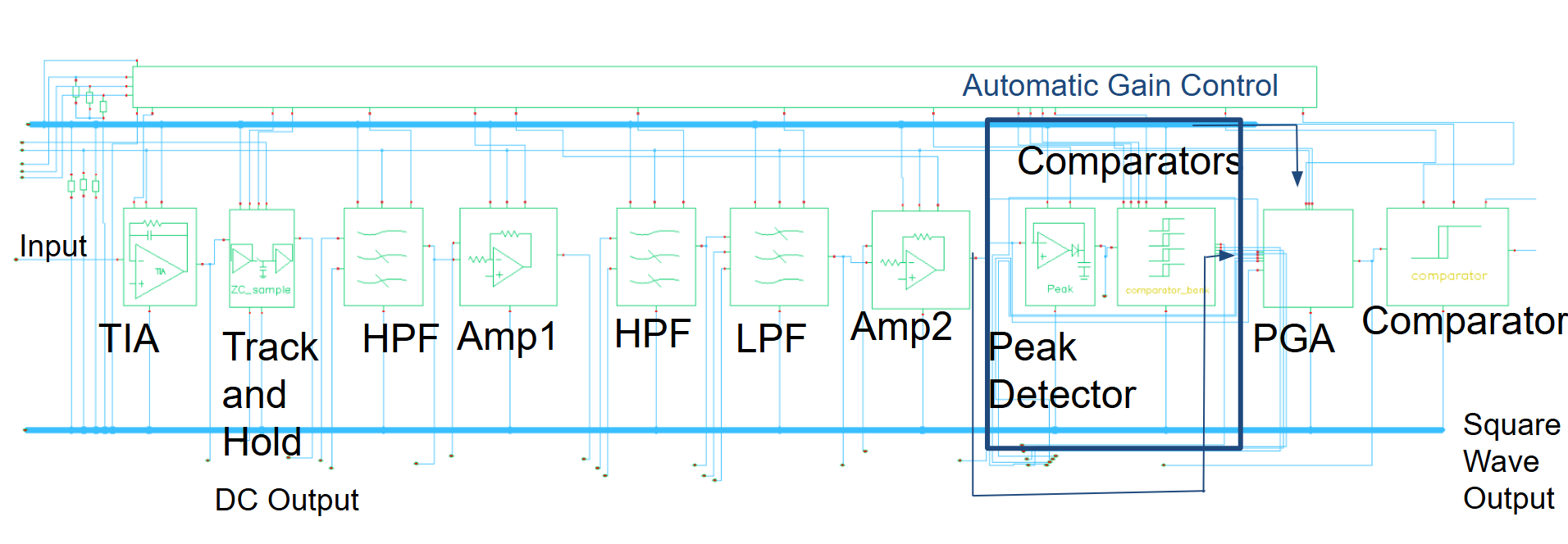
Fig 5. Block Diagram of Chip
SYSTEM TESTING
Fig. 6 shows the simulation waveforms of chip system testing under TT/27°C/VDD conditions. Fig. 6 displays the transient simulation of the overall chip (including padframe and bondwire model) when LED is pulsed at 100Hz with 10% duty cycle and track and hold is set to be 100Hz with 8% duty cycle. The duty cycle of track-and-hold is set slightly smaller than that of the LED to avoid capturing data at switching point. As can be shown, the output square waveform captures the frequency of the input AC waveform
In Fig.6, TIA_out is the output of the TIA, TH_out is the output of the track-and-hold. TIA_output alternates between 1.25V (reference voltage) when LED is turned off, and 0.75V when LED is on and there is a current. TH_out has a constant DC component of 0.75V. LPF (blue) shows the waveform after the initial high pass filter, 20dB amplifier and bandpass filter. Amp2_out shows the waveform after the second 20dB amplifier (total gain of 40dB). Peak_out detects the peak voltage of the second amplifier output. PGA_Out is the output of the PGA and is amplified by around 10dB in this schematic.
As can be seen, the system has a high settling time of around ~10s. This is due to the greater time needed to charge the capacitors to reference voltage as a result of the low duty cycle.
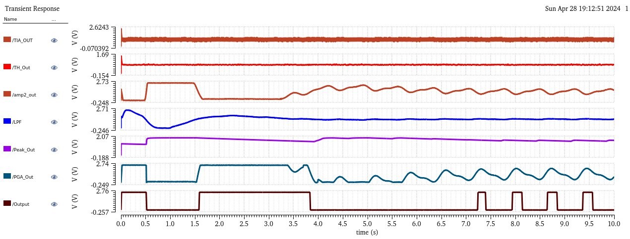
Fig 6. System Testing Transient Simulation
OTA
We utilise a two-stage OTA with Miller compensation. In addition, we have adopted a 2x sizing (width & length) for the OTAs in earlier stages to reduce noise. Miller capacitance is greater for OTAs in earlier stages to improve stability of the system.
Fig. 7 shows the OTA schematic. Sizing for input transistors is done according to gm/Id = 10.
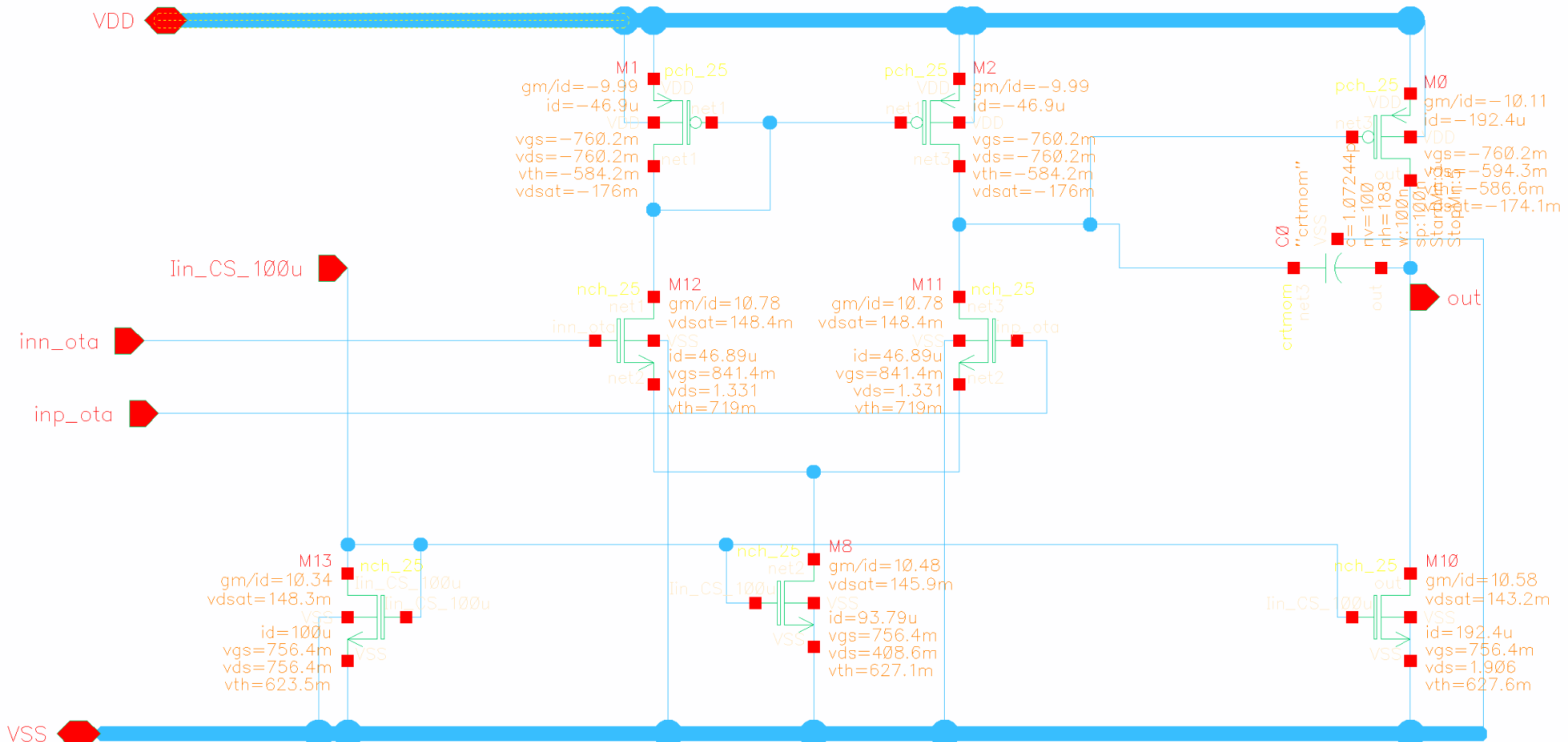
Fig 7. OTA Schematic
The following are simulation results of the OTA. Miller capacitance is around 1.2pF, and load capacitance is 1uF.
Legend: Green - TT/27°C/VDD, Blue - SS/100°C/0.9*VDD, Red - FF/0°C/1.1*VDD
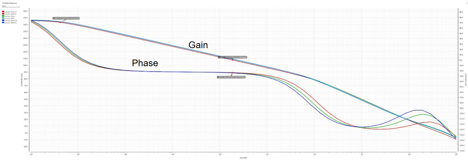
Fig 8. OTA AC Gain Open-Loop Simulation
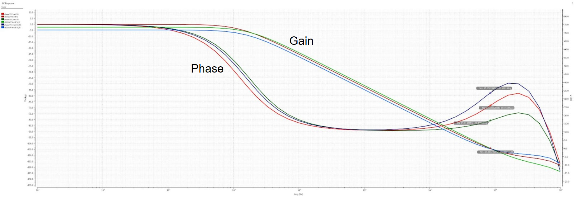
Fig 9. OTA Loop-Gain Simulation
| Performance Metrics | Value (TT) |
|---|---|
| DC Gain | 75 dB |
| Phase Margin | 62° |
| Bandwidth | 12 kHz |
| Gain-Bandwidth Product | 67 MHz |
| Slew Rate | 91 V/us |
| Max Output Current | 200 uA |
| CMRR | 69.8 dB |
Table I. 2-Stage Miller OTA Specifications
TIA
The transimpedance amplifier (TIA) converts the output current of the photodiode into voltage. The resistor of the TIA is off-chip, making the TIA gain adjustable. The TIA gain is adjusted according to the DC component of the input current, such that the voltage produced is within the input range of the chip.
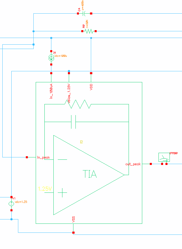
Fig 10. TIA Schematic and Testbench
The TIA OTA utilise a PMOS input differential pair to reduce noise
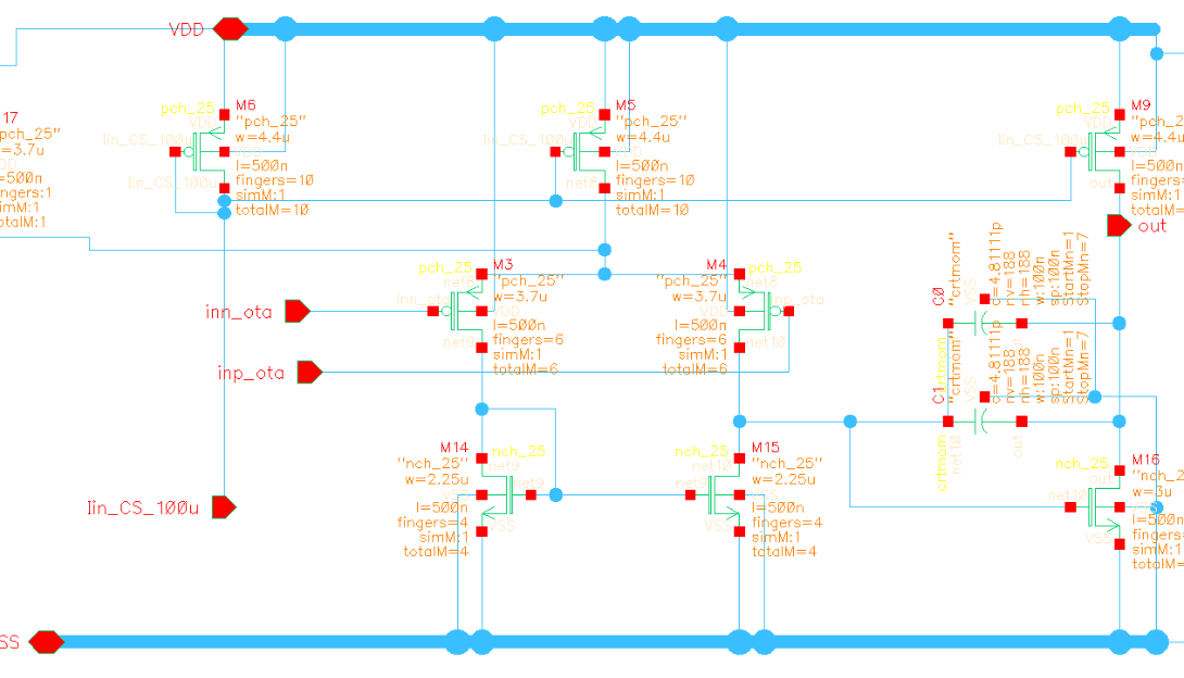
Fig 11. TIA OTA Schematic
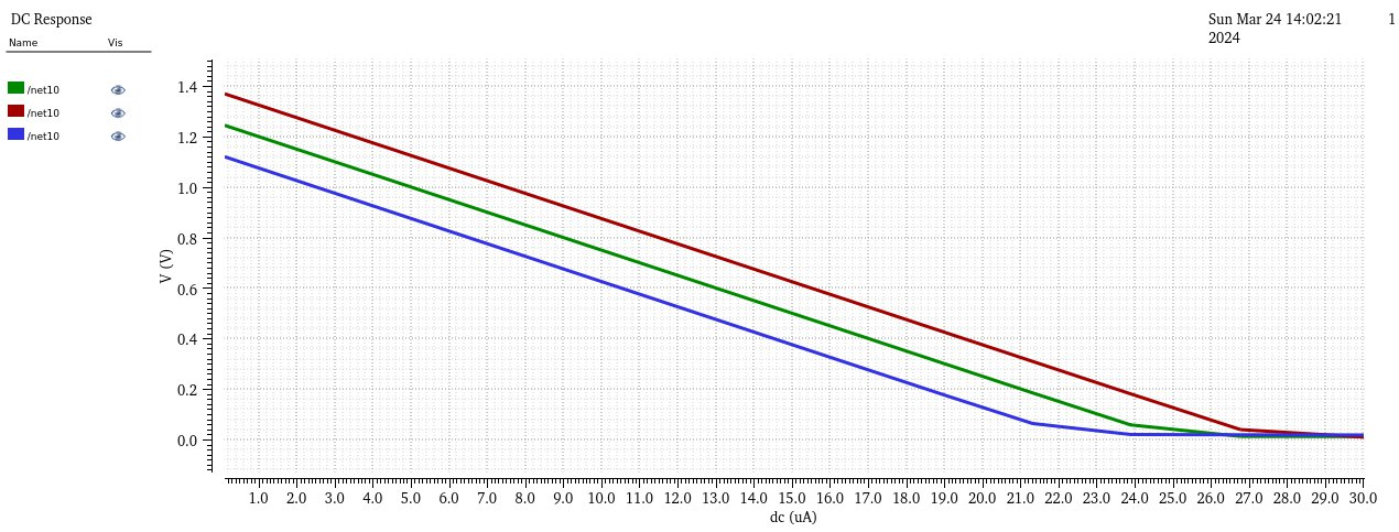
Fig 12. TIA Current-to-Voltage DC Transfer Curve
TRACK-AND-HOLD
The Track-and-Hold reads input voltage when control voltage is high and outputs stored voltage when control voltage is low.
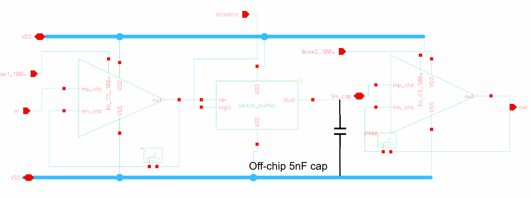
Fig 13. Track-and-Hold Schematic
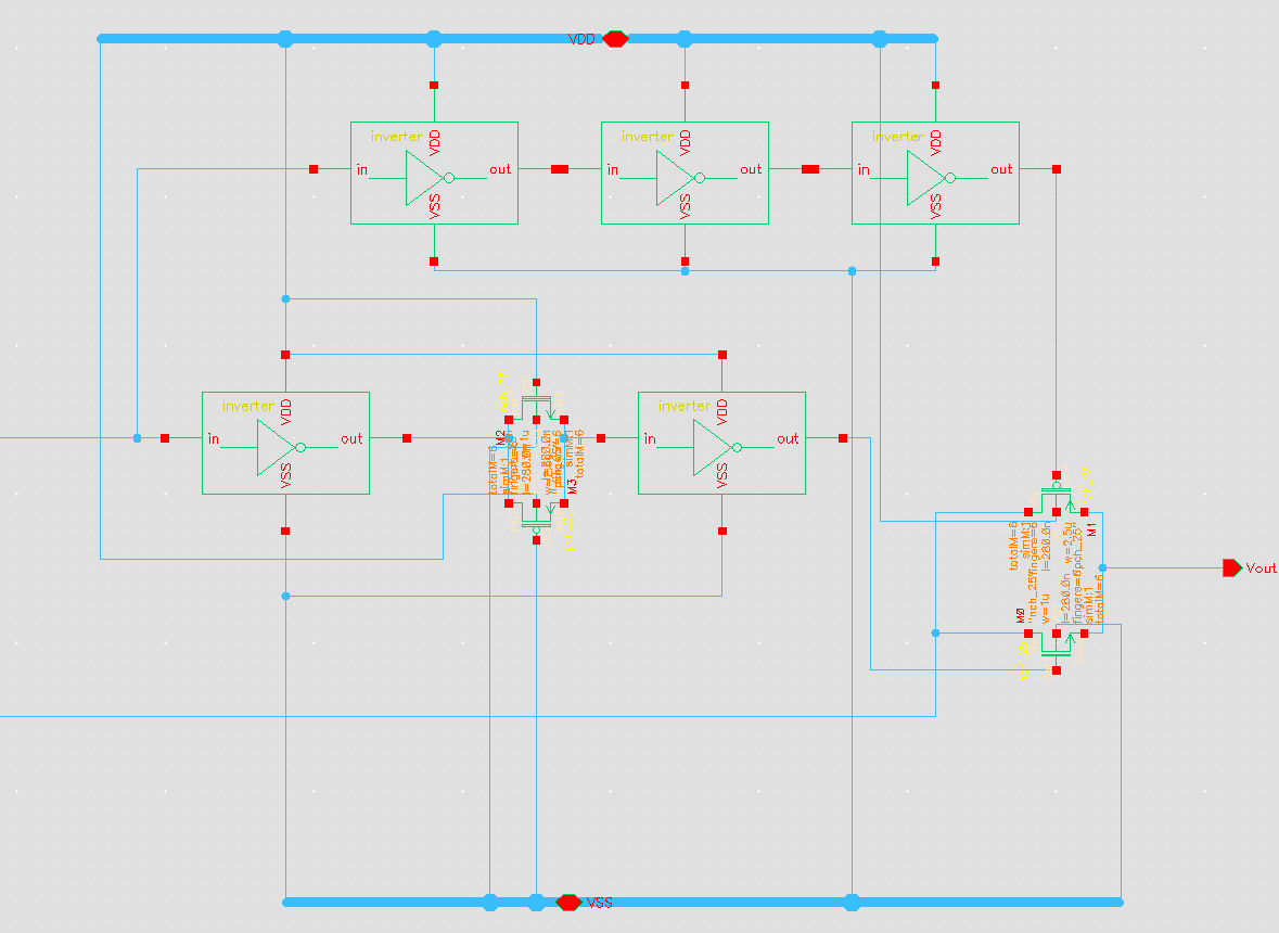
Fig 14. Schematic of Switch in Track-and-Hold
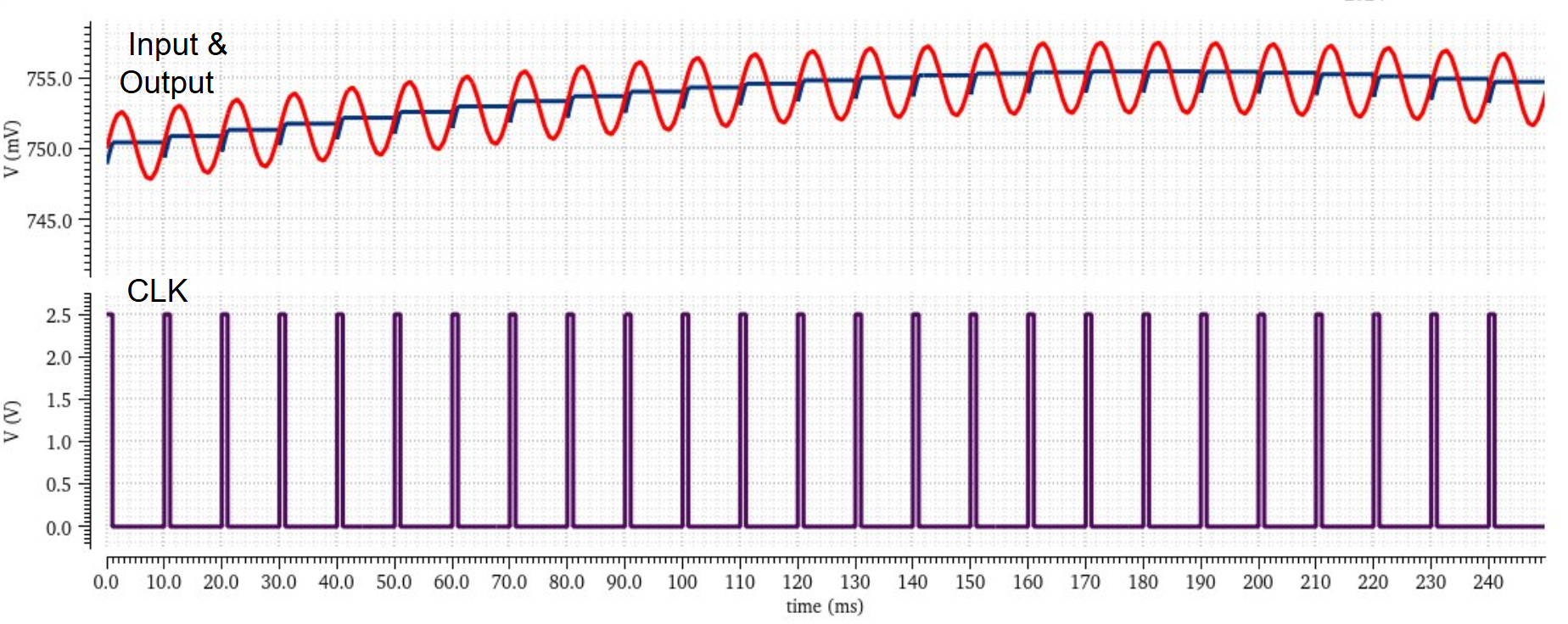
Fig 15. Track-and-Hold Transient Simulation
AMPLIFIER
The amplifier has a gain of 20dB. An additional 20 uF off-chip compensation capacitor is added in order to decrease the bandwidth of the amplifier, such that the amplifier acts as a low-pass filter. This helps to balance the load on the filters.
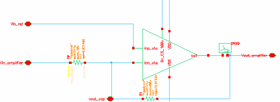
Fig 16. Amplifier Schematic
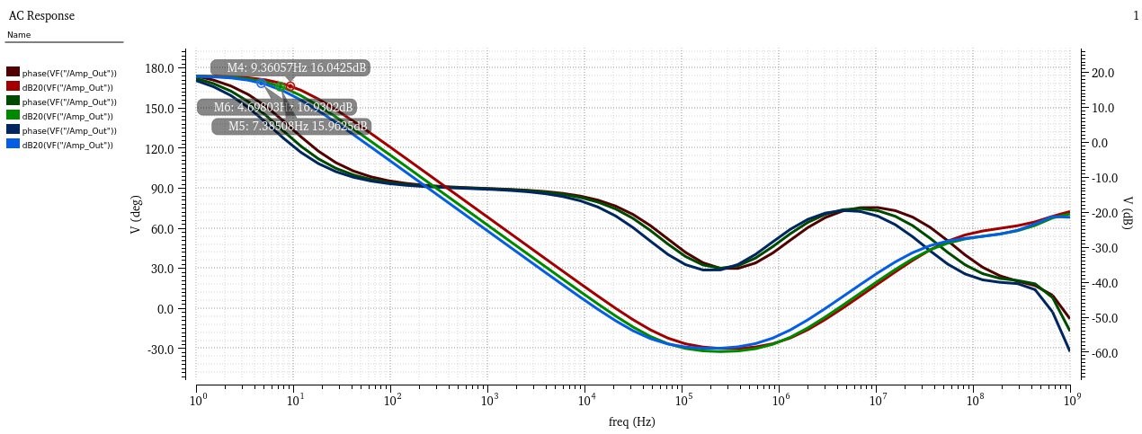
Fig 17. Amplifier Close-Loop AC Gain Analysis
HIGH-PASS FILTER
The High-Pass and Low-Pass filters both utilise the Sallen-Key topology. The Sallen-Key topology implement second-order active filters. We chose this topology as it ensures stability of the system due to its simplicity. The high-pass filter immediately after the TIA has 2x sizing in its OTA to reduce noise. The capacitors of the filters are off-chip.
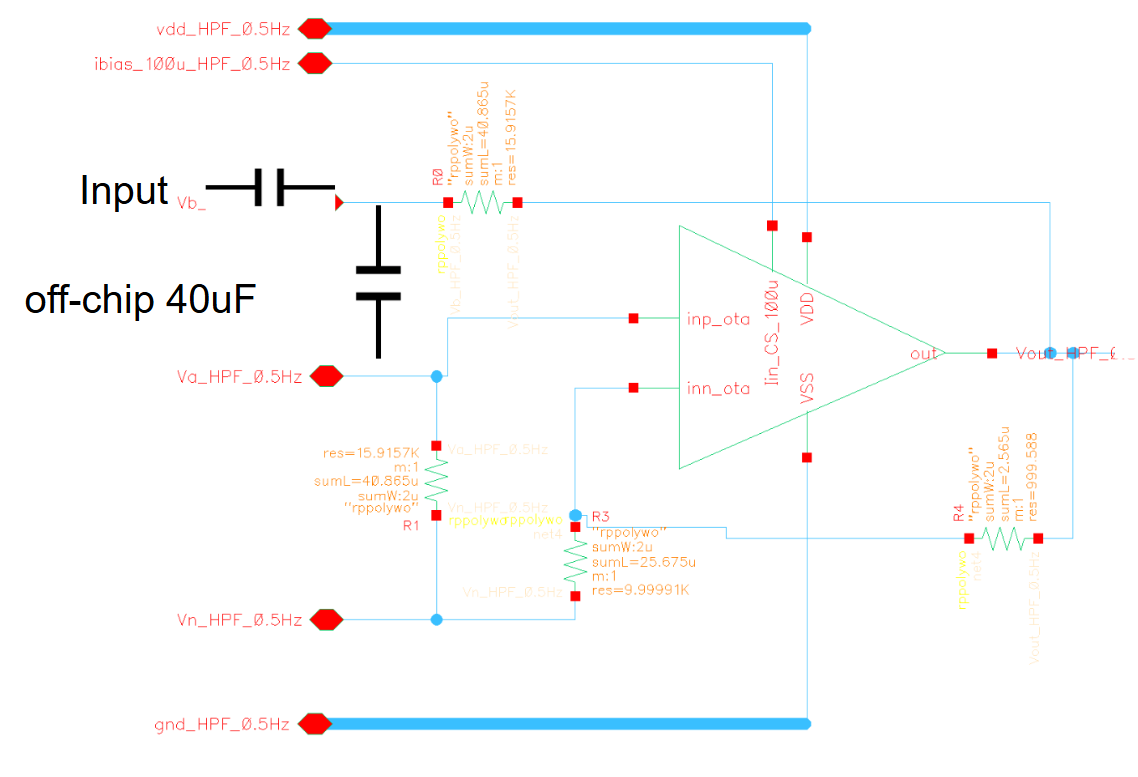
Fig 18. High-Pass Filter Schematic
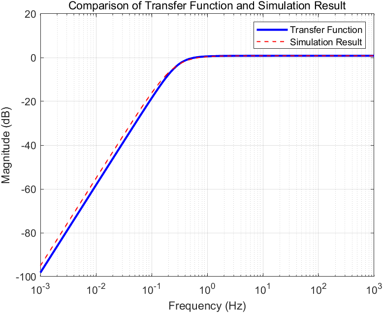
Fig 19. High-Pass Filter Simulated and Calculated AC Gain
LOW-PASS FILTER
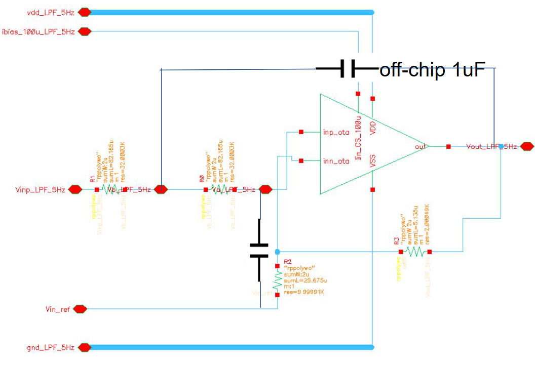
Fig 20. Low-Pass Filter Schematic
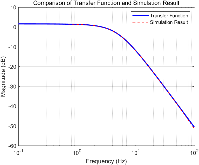
Fig 21. Low-Pass Filter Simulated and Calculated AC Gain
PEAK DETECTOR
The peak detector follows the peak of the AC waveform. This peak value is then fed back into the PGA to determine the level of amplification (feed-forward loop) such that the voltage waveform entering the comparator has an amplitude of around 0.5-1V. The off-chip capacitor is around 1uF. The RC time constant is 10, and the discharge rate of the capacitor is ~0.4V/s.
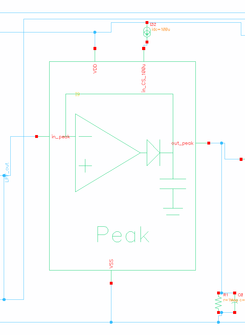
Fig 22. Peak Detector Schematic
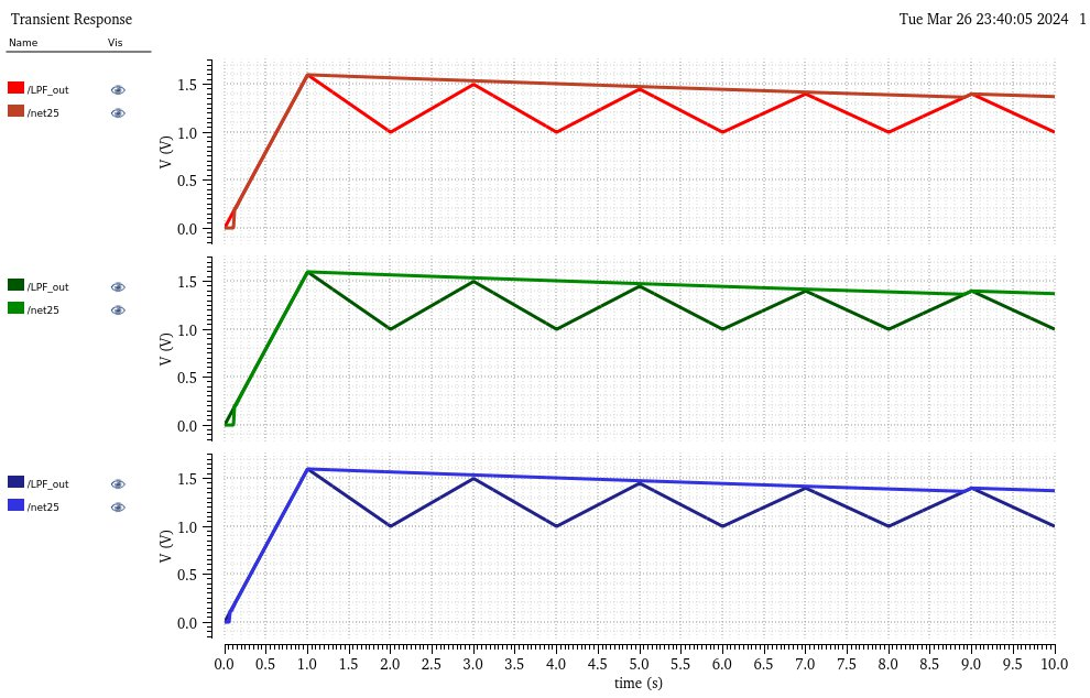
Fig 23. Peak Detector Transient Waveform
COMPARATOR
The comparator is designed to have a hysteresis voltage of around 0.11V, achieved by a use of positive feedback. The reference voltage is 1.25V.
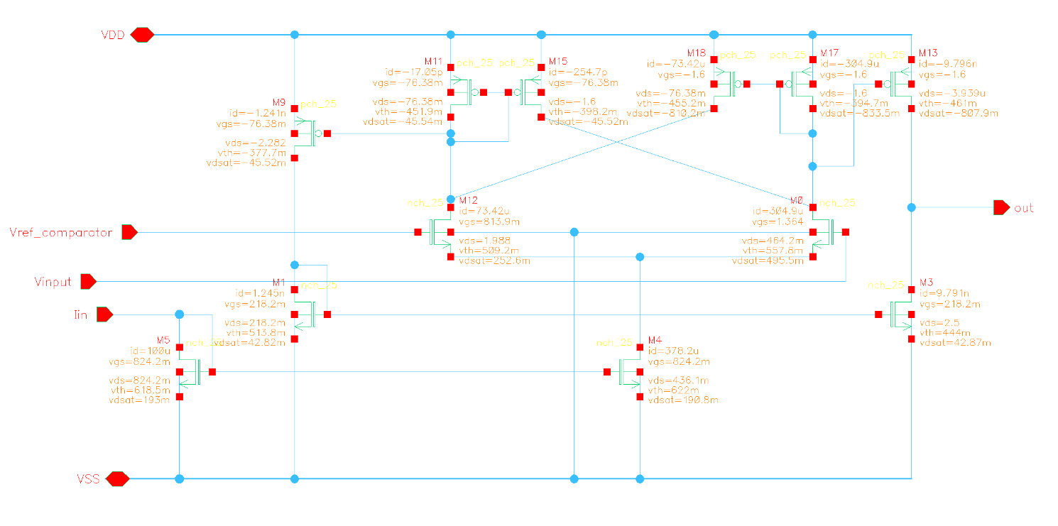
Fig 24. Comparator Schematic
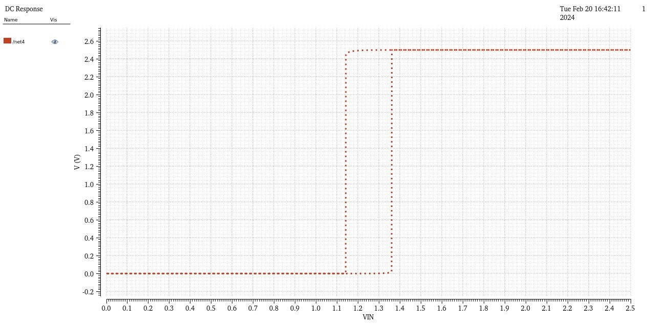
Fig 25. Comparator DC Hysteresis Sweep
COMPARATOR BANK
The comparator bank consists of four comparators and reads input from peak detector. It decides the degree of amplification by the PGA. It has 5 different modes of amplification. The logic outputs of each comparator are control voltages for the switches of the PGA.
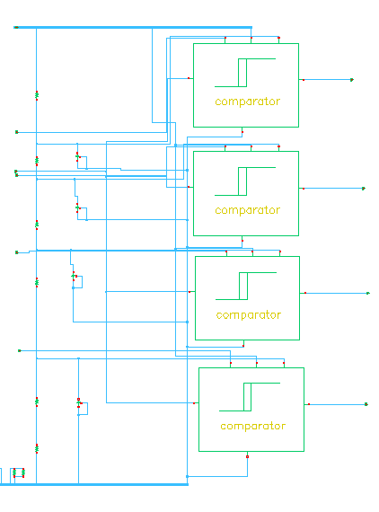
Fig 26. Comparator Bank Schematic
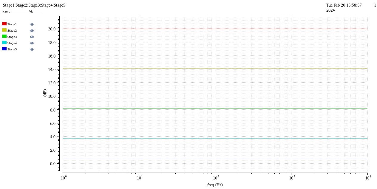
Fig 27. Comparator Bank Gain (dB) of Each Mode
PGA
The PGA has five different modes of amplication, set by the four logic outputs from comparator bank. We utilise a buffered switch design to ensure the same delay in PMOS/NMOS of the switch. For PGA switch schematic, see Fig. 14.
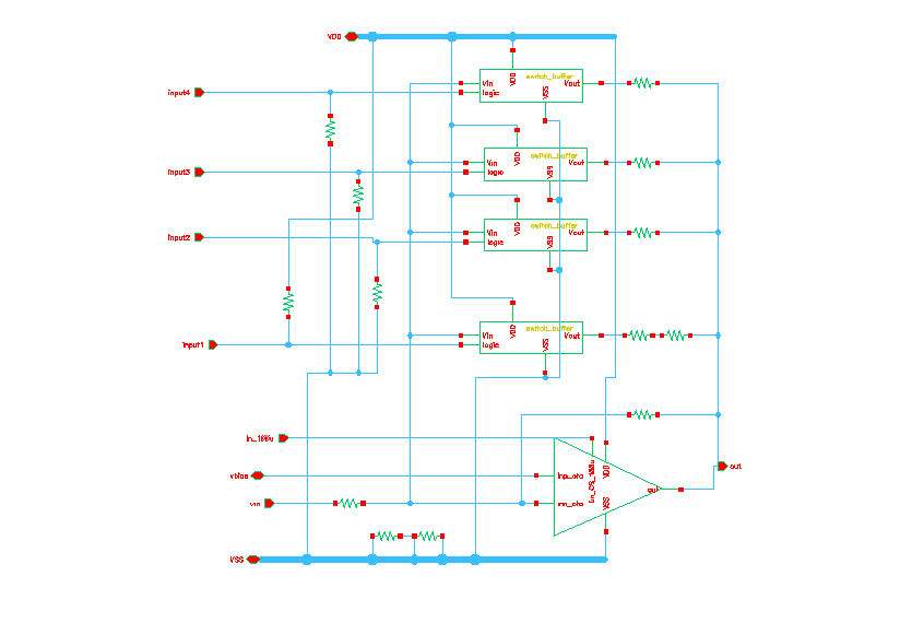
Fig 28. PGA Schematic
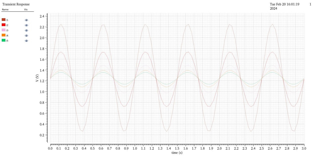
Fig 29. PGA Transient Simulation of Each Mode
| Gain Mode | Input Voltage - Reference Voltage (V) | Gain (dB) |
|---|---|---|
| 1 | 0 - 0.08 | 20 |
| 2 | 0.08 - 0.25 | 14.1 |
| 3 | 0.25 - 0.5 | 8.2 |
| 4 | 0.5 - 0.8 | 3.8 |
| 5 | 0.8-1.25 | 0.8 |
Table II. PGA Gain Modes
CURRENT BANK
The current bank takes in three different reference currents as input, for TIA, all comparators, and the rest of the OTAs. Each reference current is designed to be 100uA, and the input currents are separated for ease of adjustment during testing phase.
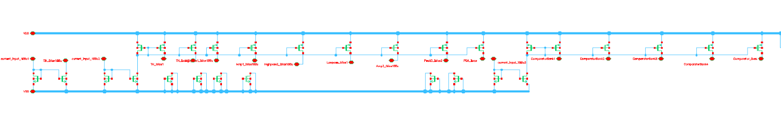
Fig 30. Current Bank Schematic