
LAYOUT DESIGN
TOP-LEVEL LAYOUT WITH PADFRAME
The top-level layout design is shown in Fig. 31. Decoupling capacitors were placed for reference voltage line, VDD line, and the bias currents. Metal filling over the capacitors are done in higher metal layers.
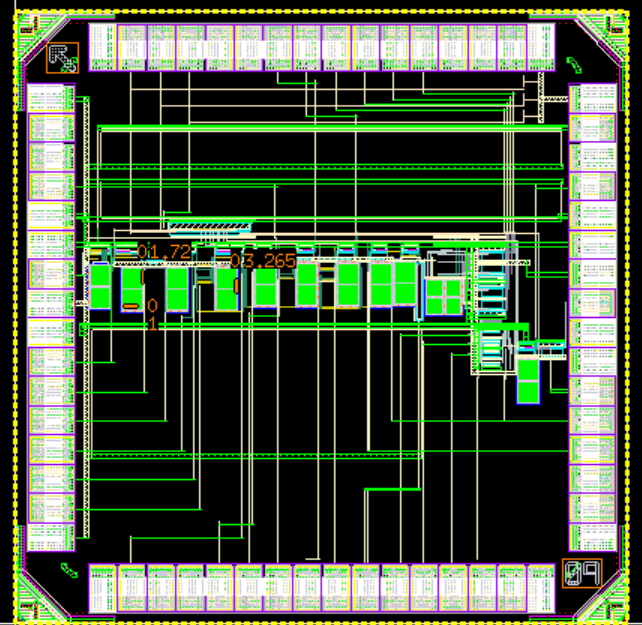
Fig 31. Top-Level Layout
TIA
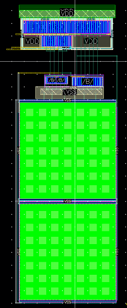
Fig 32. TIA Layout
TRACK-AND-HOLD
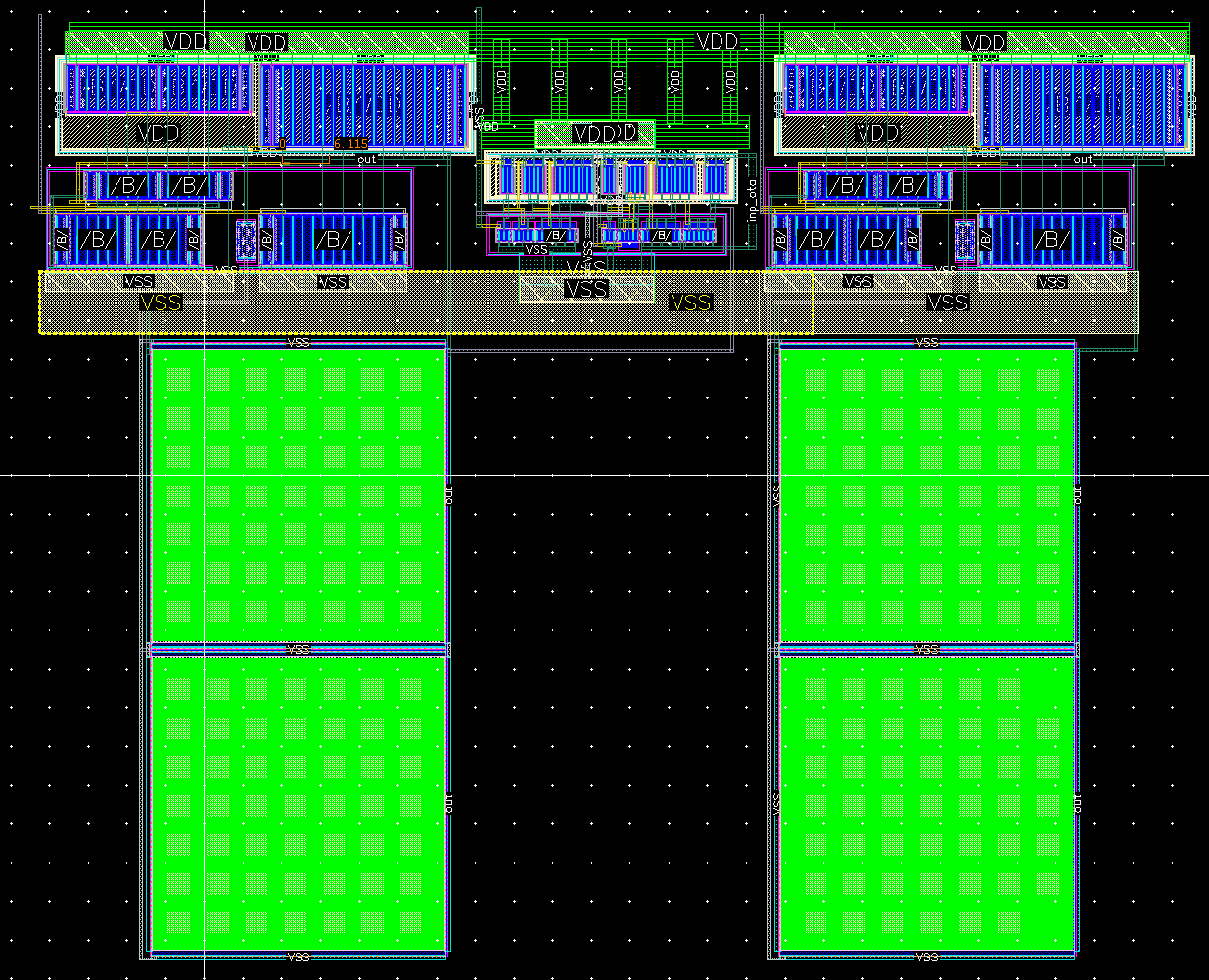
Fig 33. Track-and-Hold Layout
HIGH-PASS FILTER
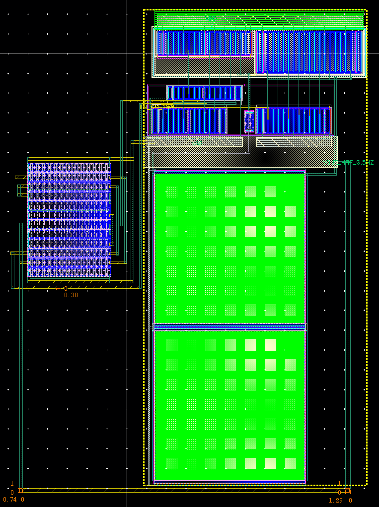
Fig 34. High-Pass Filter Layout
AMPLIFIER
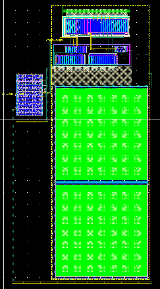
Fig 35. Amplifier Layout
LOW-PASS FILTER
Fig 36. Low-Pass Filter Layout
PEAK DETECTOR
Fig 37. Peak Detector Layout
COMPARATOR
Fig 38. Comparator Layout
COMPARATOR BANK
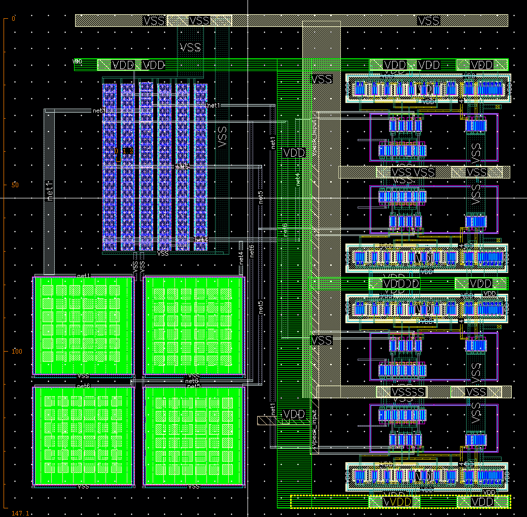
Fig 39. Comparator Bank Layout
PGA
Fig 40. PGA Layout
CURRENT BANK
Fig 41. Current Bank Layout