EE6350 VLSI Design Lab
Spring 2023
Digital Clock
Xueji Zhao
Tianyu Qin
Xinyuan Fu
Gehui Liang
|
Introduction
|
System Overview
|
IC Design
|
IC Layout
|
PCB Design
|
Testing Result
|
Conclusions
|
Acknowledgements
|
PCB Design
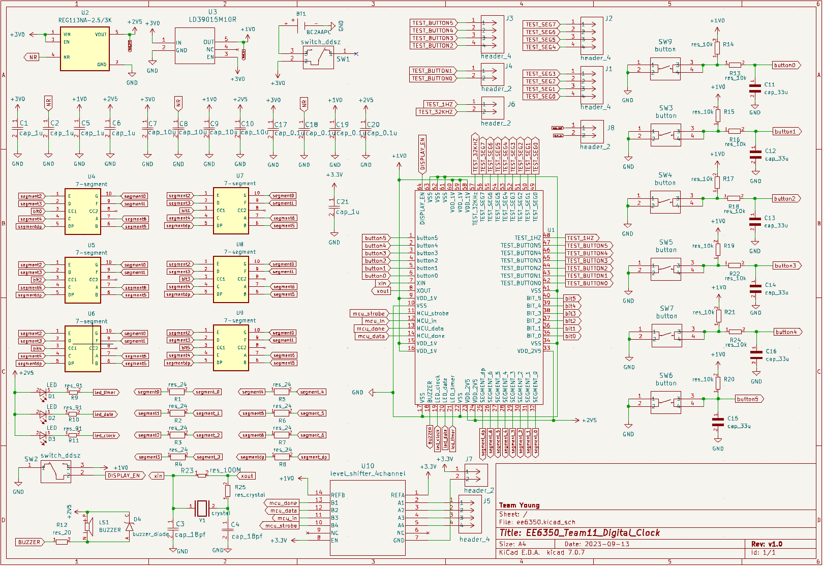
Fig 1. PCB Schematic
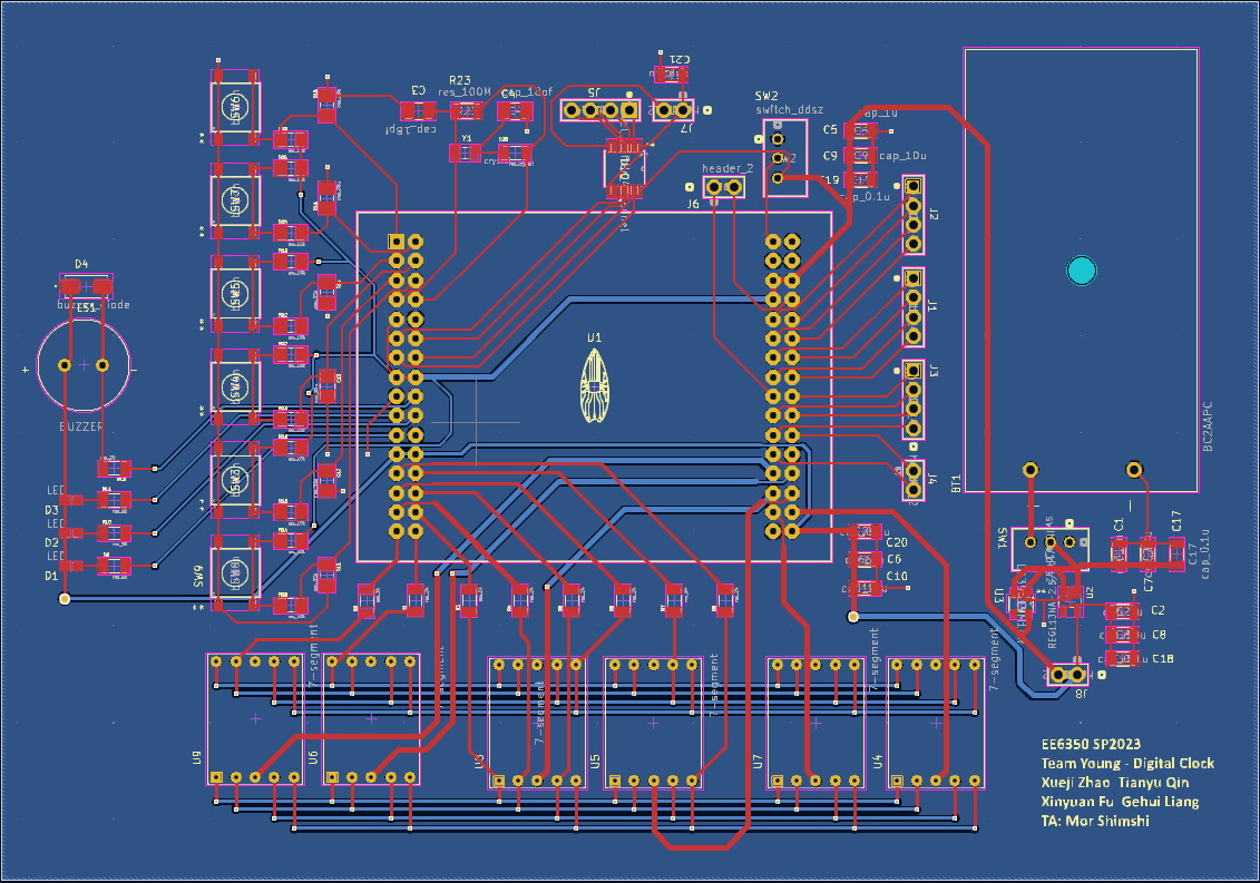
Fig 2. PCB Layout
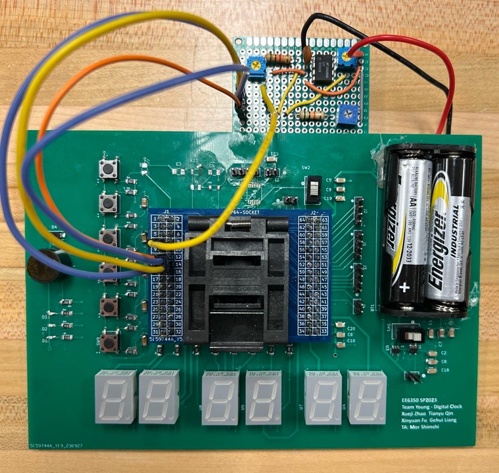
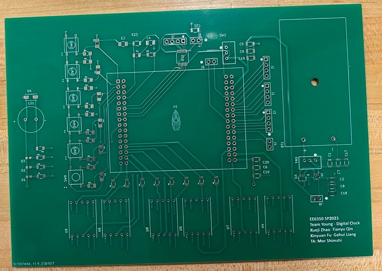
Figure 3 and 4 shows the front and back of the complete PCB board.
Fig 3. PCB Board Front
Fig 4. PCB Board Back
Back to top