
PCB Design
The whole chip pin diagram is shown in Figure. 1. The whole chip is divided into two parts, the upper side is the SAR ADC part(1-12, 37-64). The second part is the DAC part(13-36). The Figure. 2 shows the physical picture of the chip.
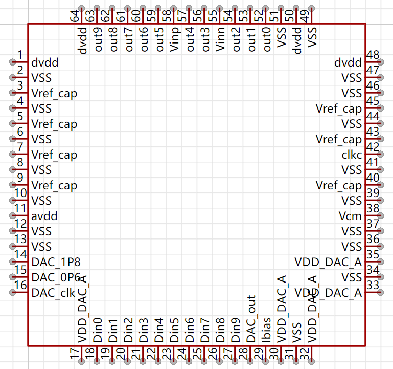
Figure. 1 Pin Diagram
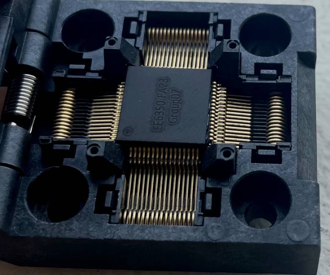
Figure. 2 The Physical Picture of the Chip
To realize the function of a sound card, we use a PCB to give proper voltage supply and voltage reference. Meanwhile, we add several pins to give sufficient space so that we can hook up the test pin with various measurement instruments, such as an oscilloscope. The PCB also has a single-ended to differential output amplifier to convert audio signal input. Eventually, the output of DAC would be connected to a class-d amplifier before the speaker. Figure. 3 is the 3D preview of our design PCB with components soldered. Figure. 4- Figure. 6 illustrates the schematic design of the whole PCB.
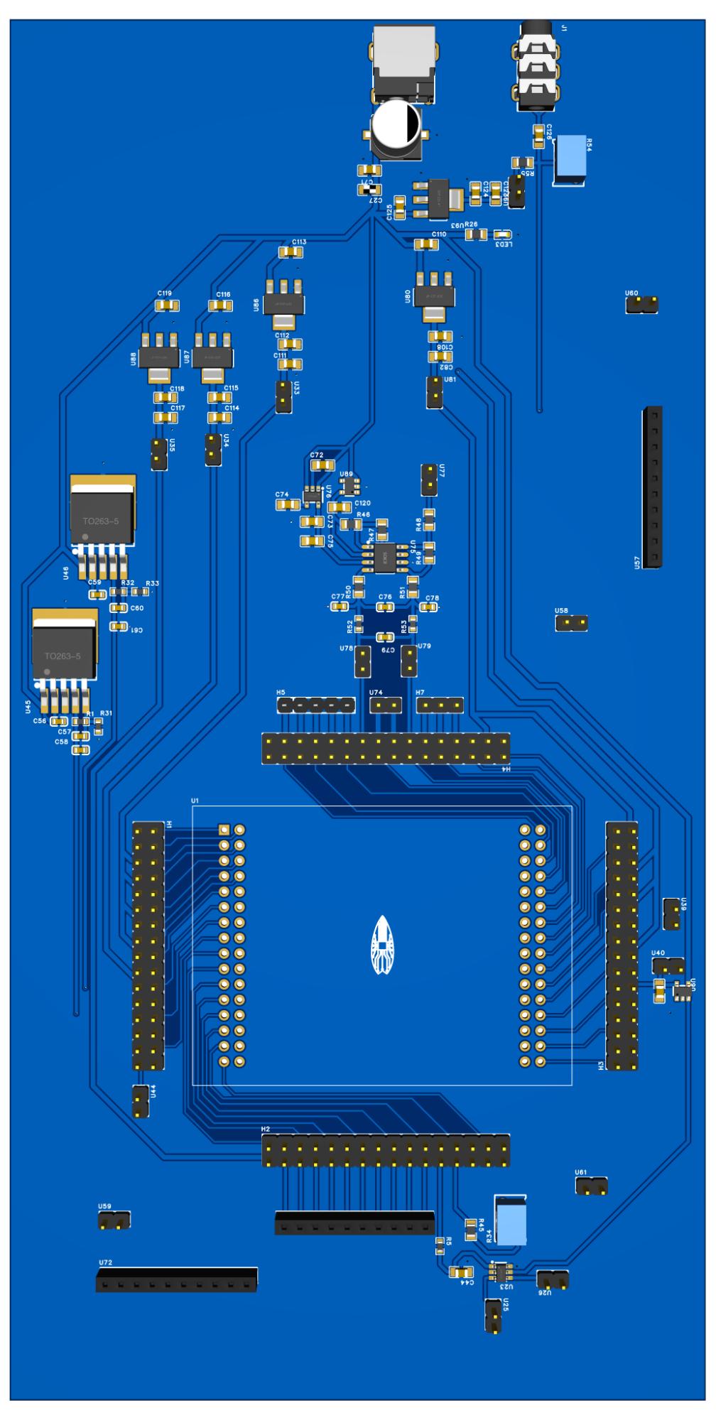
Figure. 3 PCB Board Design 3D Preview
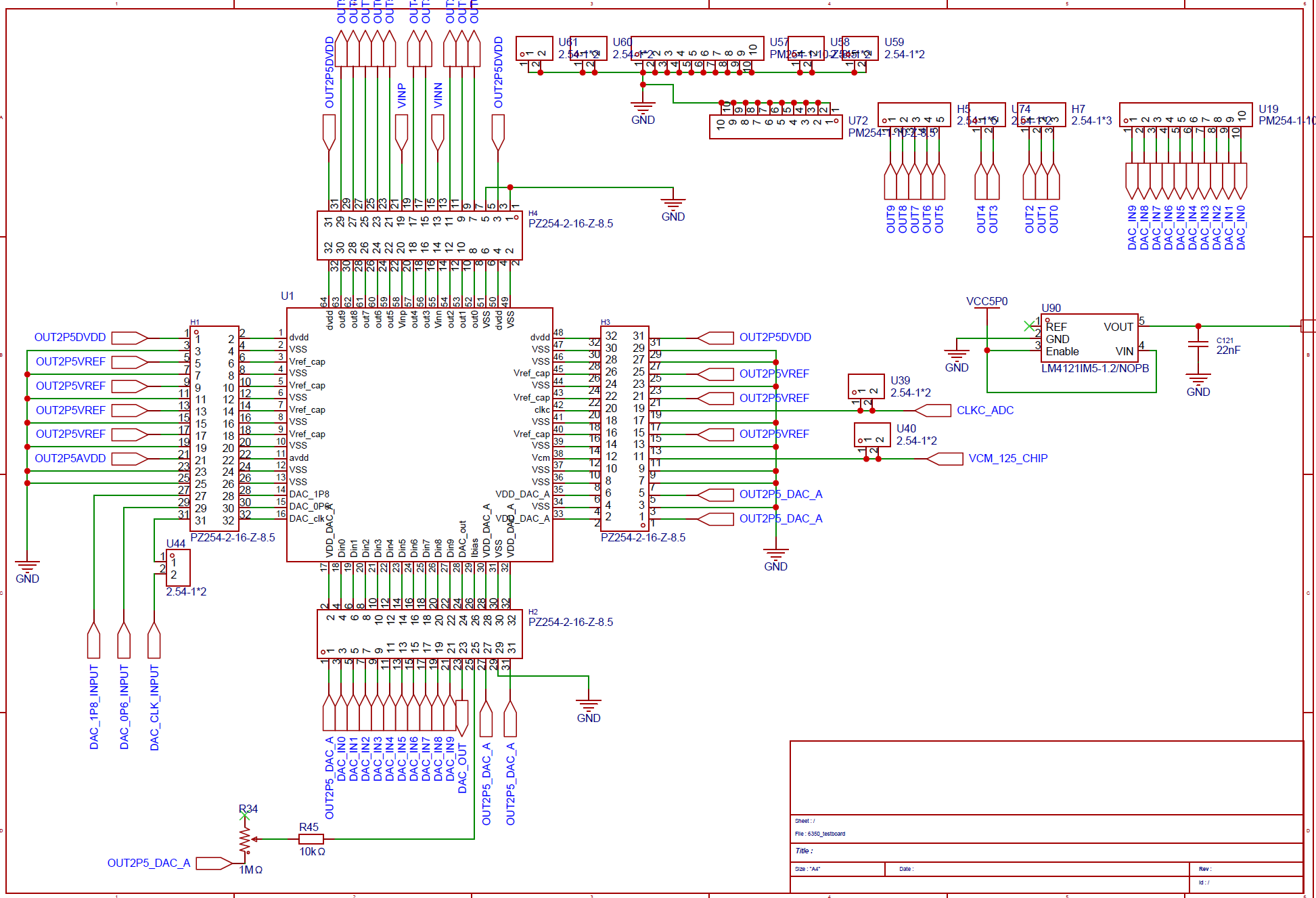
Figure. 4 Top Level Schematic of PCB
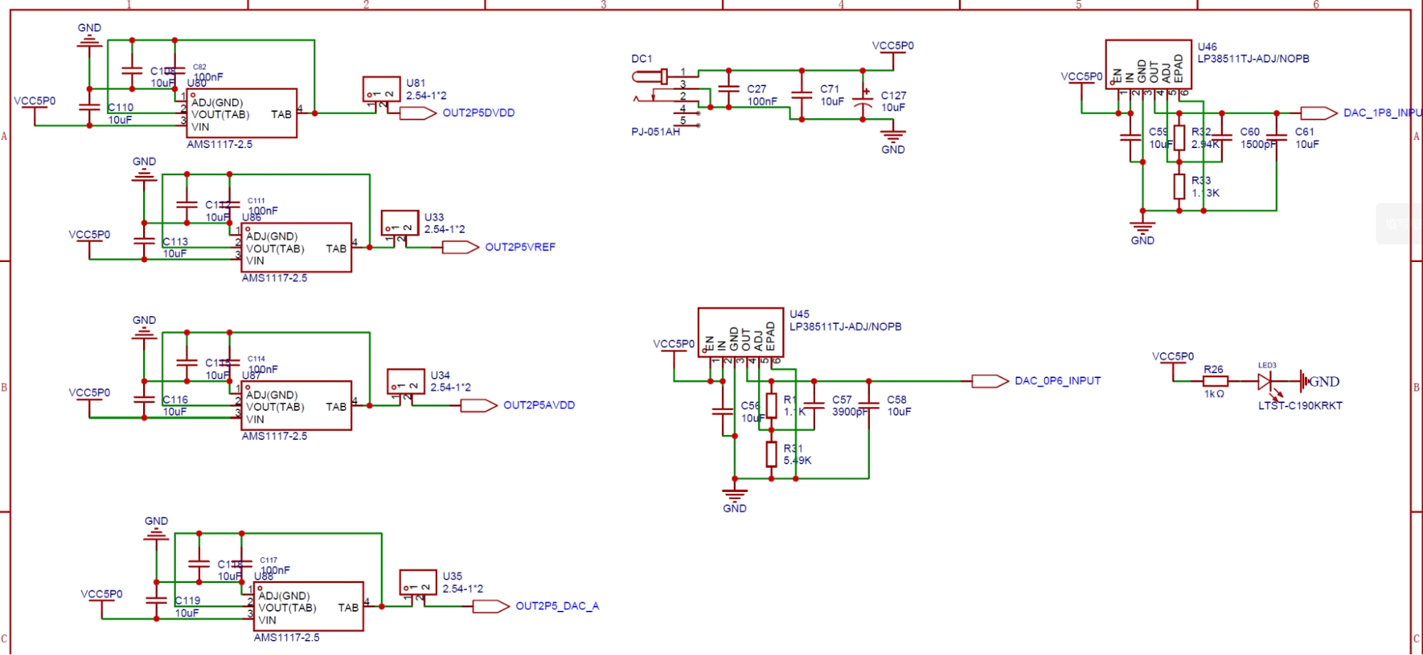
Figure. 5 Power Supply Schematic of PCB
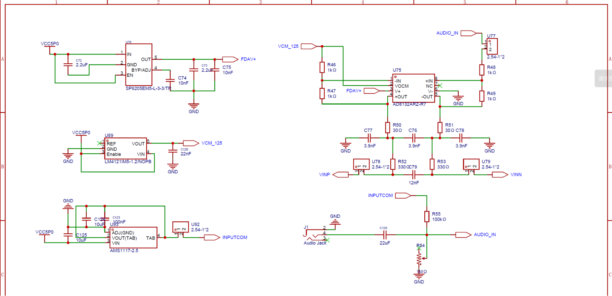
Figure. 6 Single-ended Input to Differential Output Schematic of PCB