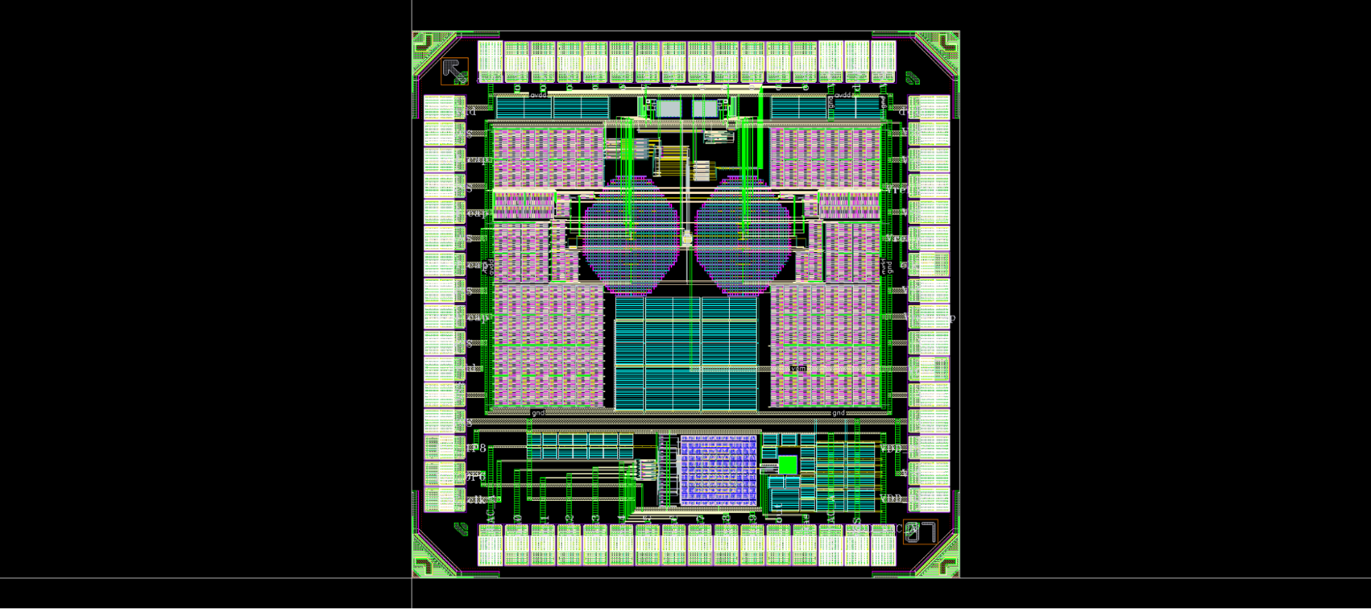
IC Layout
ADC LAYOUT
Sample/Hold Circuit
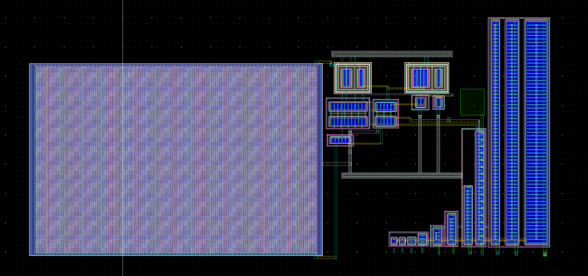
Figure. 1 The Layout of S/H Circuit
Frequency divider Circuit
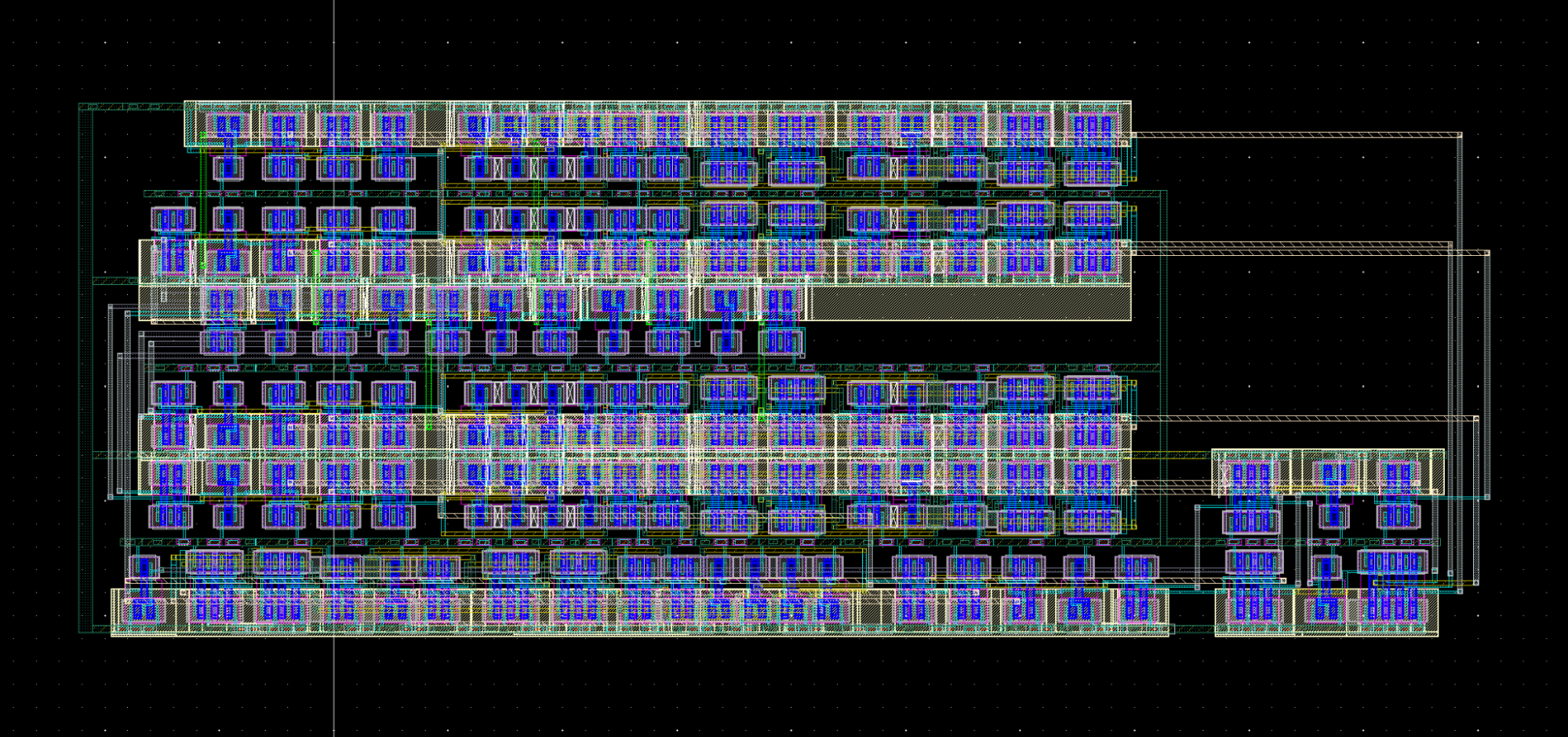
Figure. 2 The Layout of Frequency Divider Circuit
Strong-Arm Comparator
We try to use symmetric structure and dummy mos to decrease the impact of mismatch and STI effect.
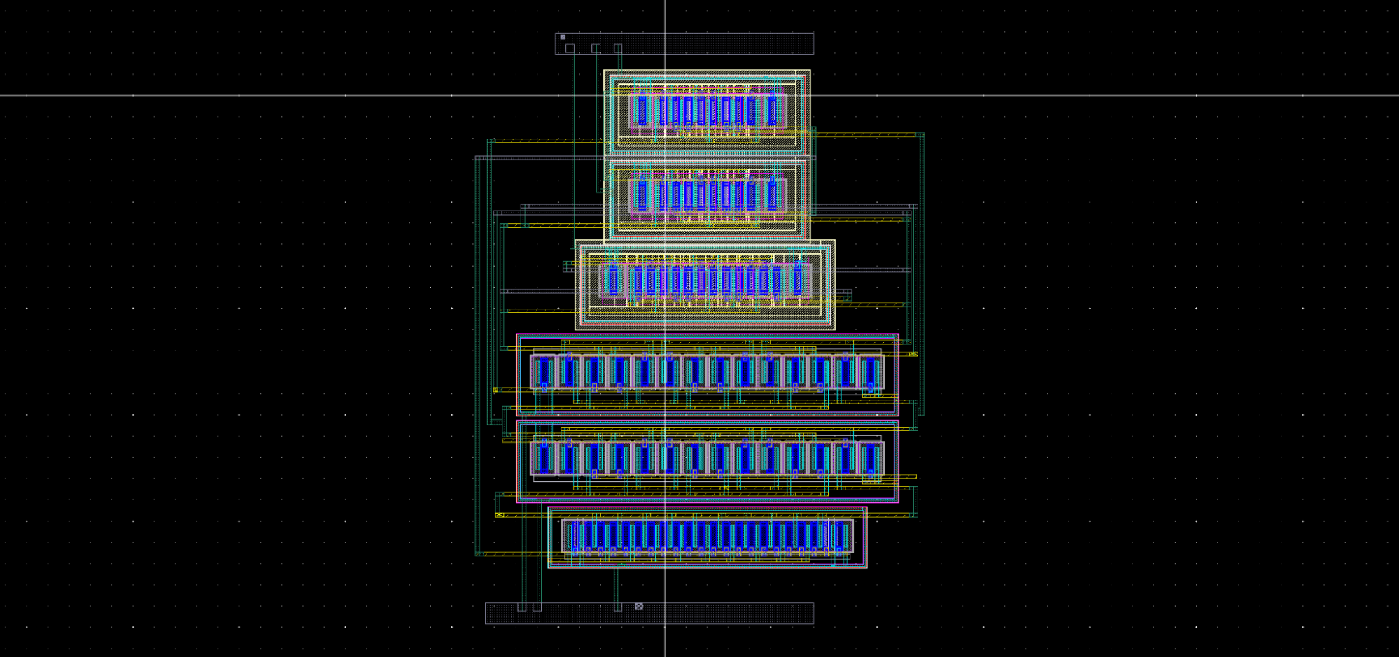
Figure. 3 The Layout of Strong-Arm Comparator
10-bit Capacitor DAC & Switch
The single unit switch layout. The whole capacitor array uses the common-centroid method. The overall layout of the combination of switch and dac for one half.

Figure. 4 The Layout of Unit Capacitor DAC Switch
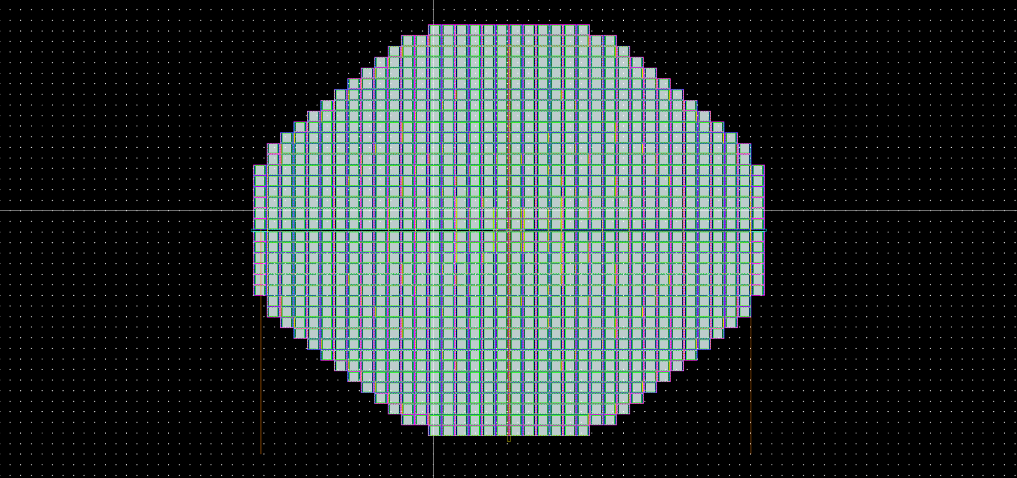
Figure. 5 The Layout of Capacitor Array
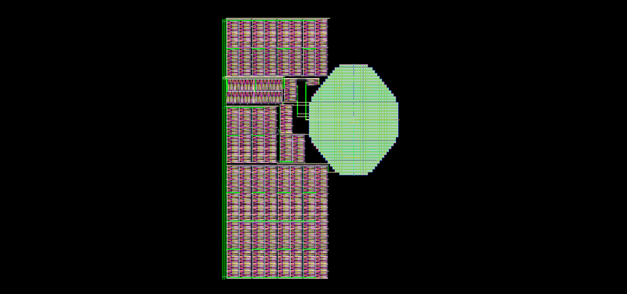
Figure. 6 The Layout of Switch and Capacitor Array
SAR logic block
Here is the SAR logic block layout, the shifter would be the left side and the delay line is in the middle. The left part is the register used to store the result from the comparator.
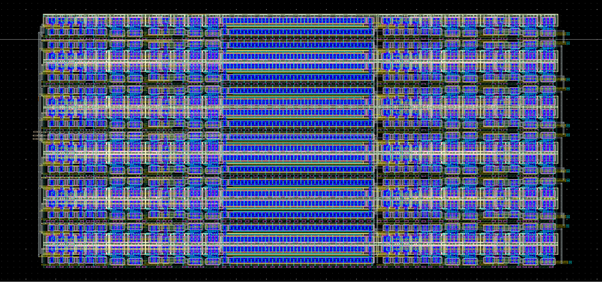
Figure. 7 The Layout of SAR Logic Block
Top level layout of ADC
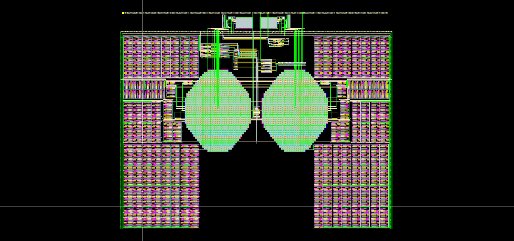
Figure. 8 The Layout of ADC
DAC LAYOUT
Input register
The input register is composed of 10 D flip-flops arranged side by side.
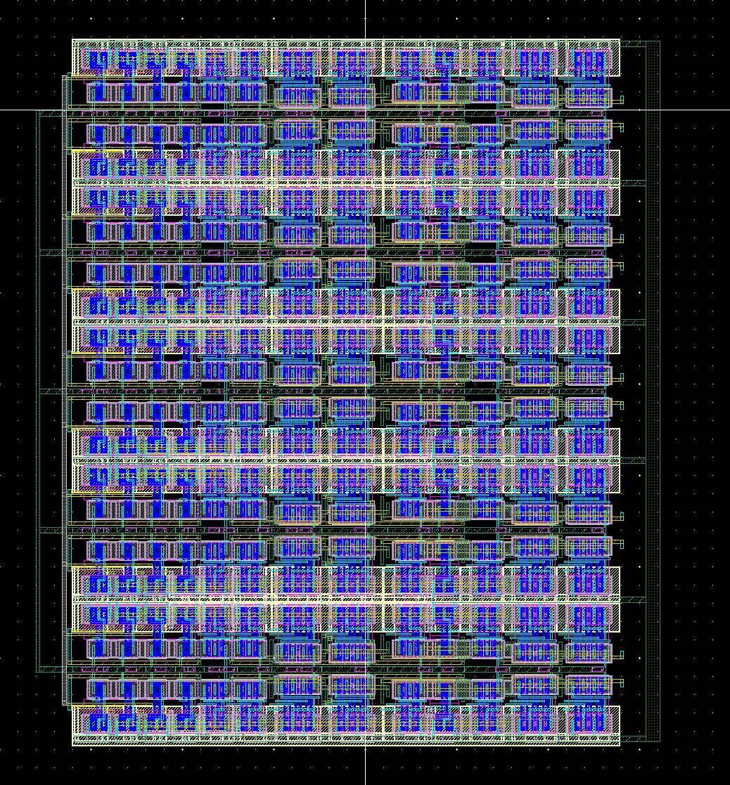
Figure 9. Layout of 10 bit input register
10 bit switches
Ten switches are placed in parallel, sharing vdd and gnd pad.
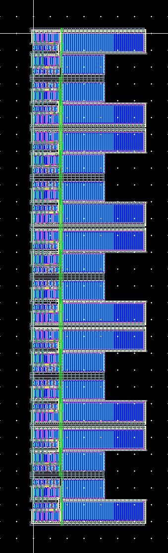
Figure 10. Layout of 10 bit switch
R-2R array
The most critical issue in the layout design of an R-2R DAC is the matching of resistors. Since the output value of an R2R entirely depends on the resistor values, a large mismatch between the resistors for each bit can lead to significant deviations in the voltage output. To enhance the matching of resistors and reduce the mismatch among on-chip resistors, we have adopted a centroid layout structure. For achieving a symmetrical structural design, each R is split into two equal resistor cells. Similarly, each 2R is divided into four equal resistor cells. As shown in the diagram, each resistor cell is symmetrically placed to minimize mismatch.
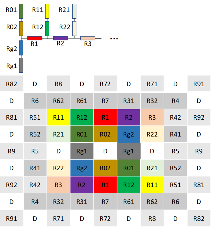
Figure 11. Layout plan for centroid R array
As a result, in the layout, the value for each resistor is R/2. Furthermore, to balance the resistor of each bit, the resistance of wires connected on each bit is taken into consideration.
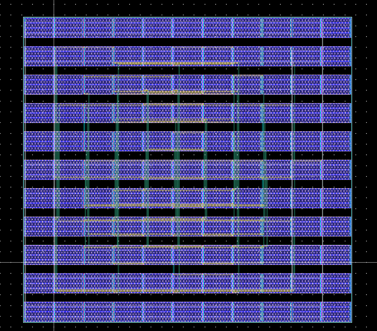
Figure 12. Centroid layout of R2R array
Output buffer op amp
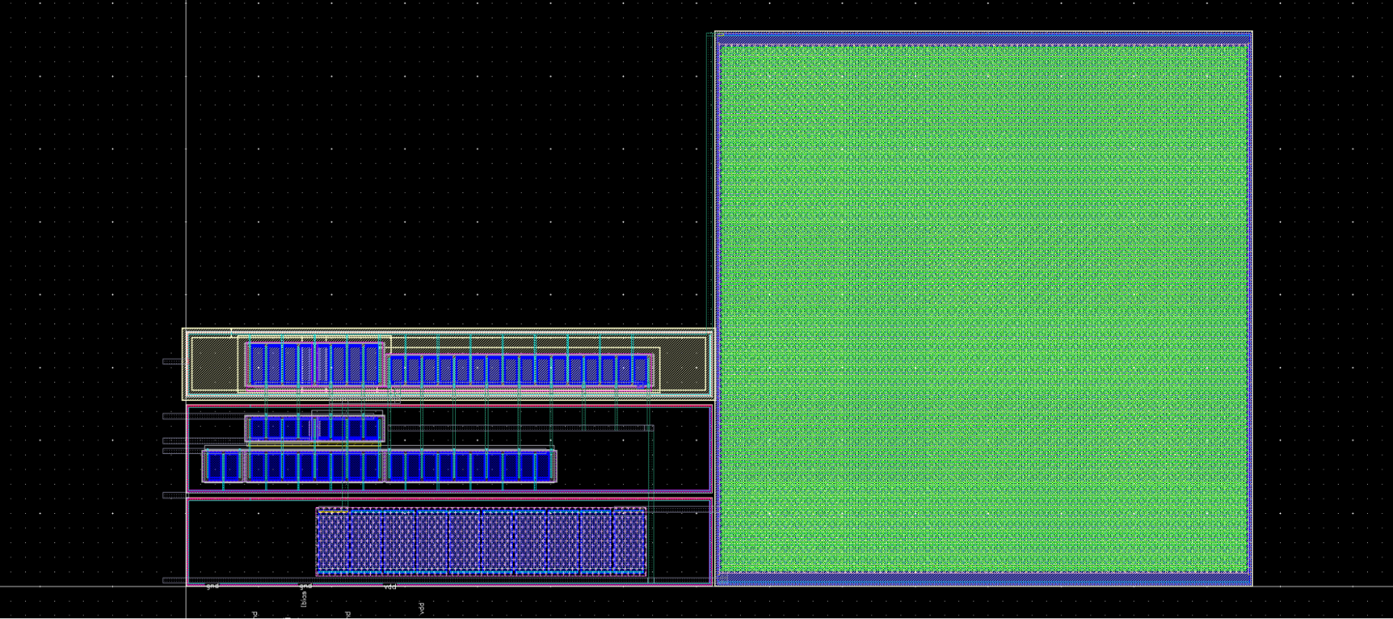
Figure 13. Layout of 2-stage opamp
Top level layout of DAC
After all blocks passing DRC and LVS, they are placed together. The signal flow of DAC goes from left to right, with vdd at the top and gnd at the bottom.
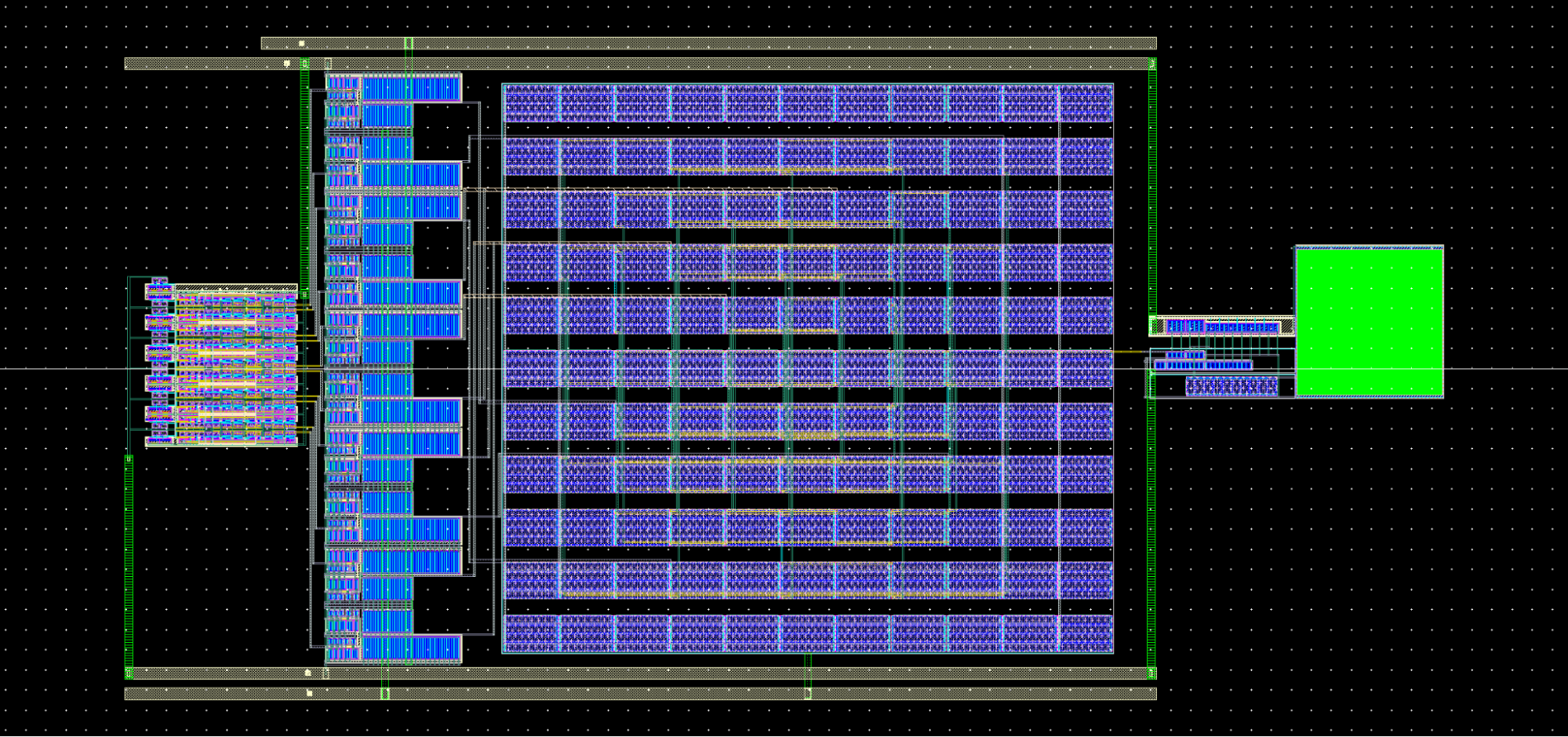
Figure 14. Top level layout of the DAC
CHIP LAYOUT