
IC Design
Transistor Level Design
The 10-bit SAR ADC can be divided into five blocks including Sample/Hold block, Comparator, 10-bit Capacitor DAC & Switch, SAR logic block and timing block. We would like to show more details for each block.
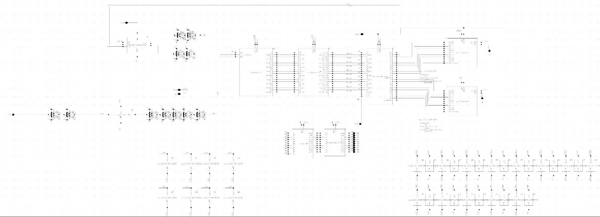
Figure. 1 Top Level Schematic for SAR ADC
Sample/Hold Circuit
In the design of the ADC sampling circuit, we have chosen the bootstrapped sampling switch circuit for implementation. This sampling circuit precharge a “boosting” capacitor CB to VDD. When the switch is on, this capacitor will set the VGS of the sampling switch to VDD, regardless of the input voltage. By adjusting the W/L of the sampling MOSFET, we can ensure that the Hold Pedestal of each sampling bit is consistent. This design structure has the following benefits
1. Enhanced Accuracy: The bootstrapped switch, by maintaining a stable voltage at the switch node, reduces variations in switch resistance, thereby enhancing the accuracy of the ADC.
2. Reduced Non-linear Distortion: In high-speed ADCs, variations in switch resistance can lead to non-linear distortion. The bootstrap circuit helps reduce this distortion, which is particularly important in high-resolution applications like 10-bit sampling.
3. Support for High Sampling Rates: The use of a bootstrapped switch allows for more efficient handling of high-speed signals, enabling the circuit to operate stably at a sampling rate of 100k.
4. Improved Dynamic Range: The dynamic range refers to the ratio of the smallest to the largest signal the circuit can process. In high-resolution ADCs, improving the dynamic range means more accurately capturing signals from faint to strong.
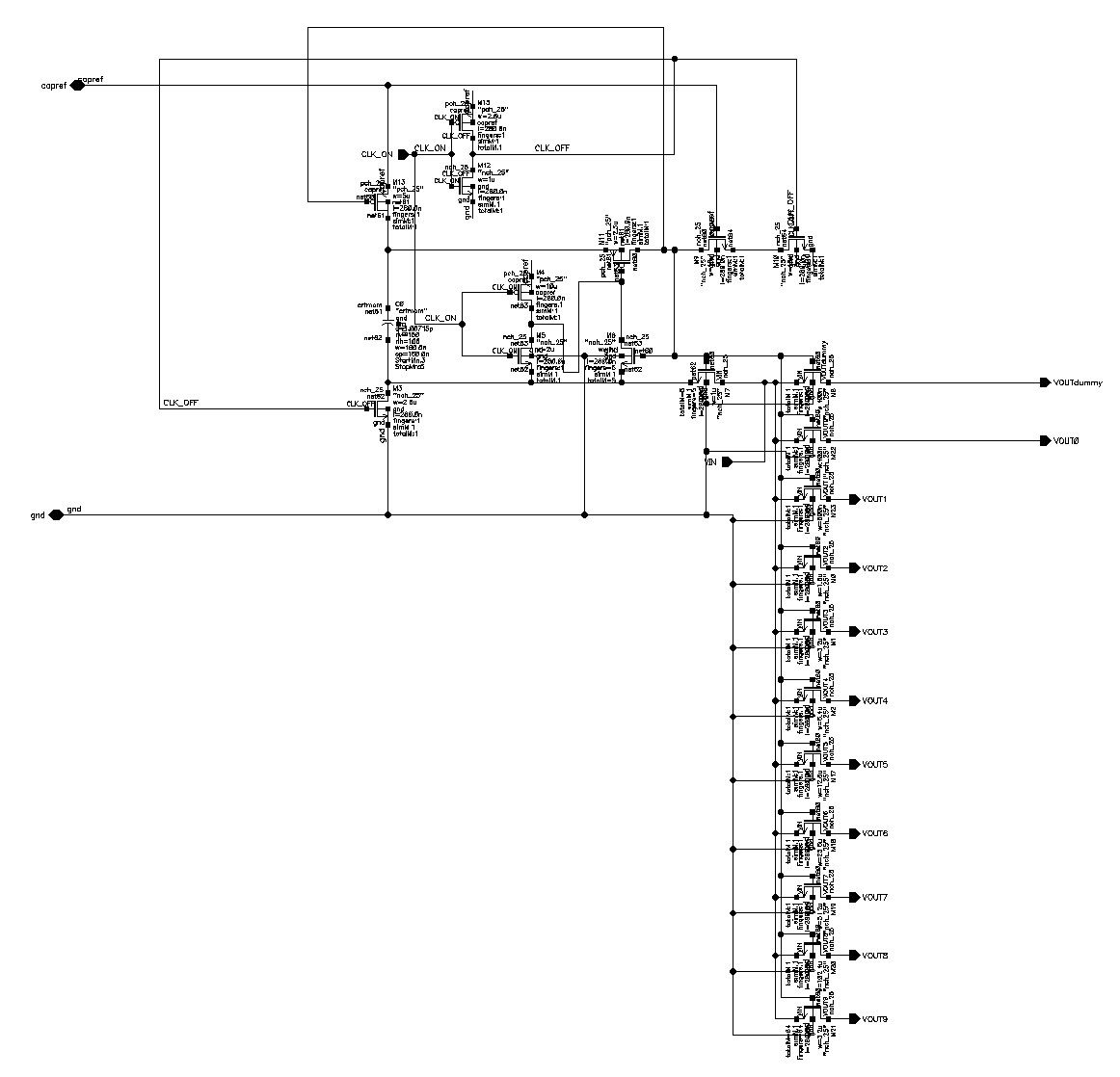
Figure. 2 The schematic of S/H circuit
Frequency divider Circuit
Sampling for 10 cycles may result in the last bit not having time to store the comparison results. So we set up 11 sampling cycles to complete the comparison and store the results. Our clock frequency is 2.2MHz and the sampling frequency is 100kHz, so we have designed an 11 division circuit to achieve this function. We use a counter composed of a JK trigger, which flips the counting direction once every time it reaches 11 and outputs a signal to the external digital logic.
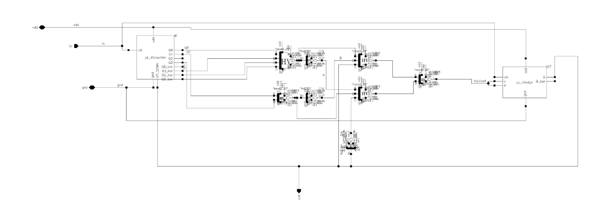
Figure. 3 The schematic of Frequency divider Circuit
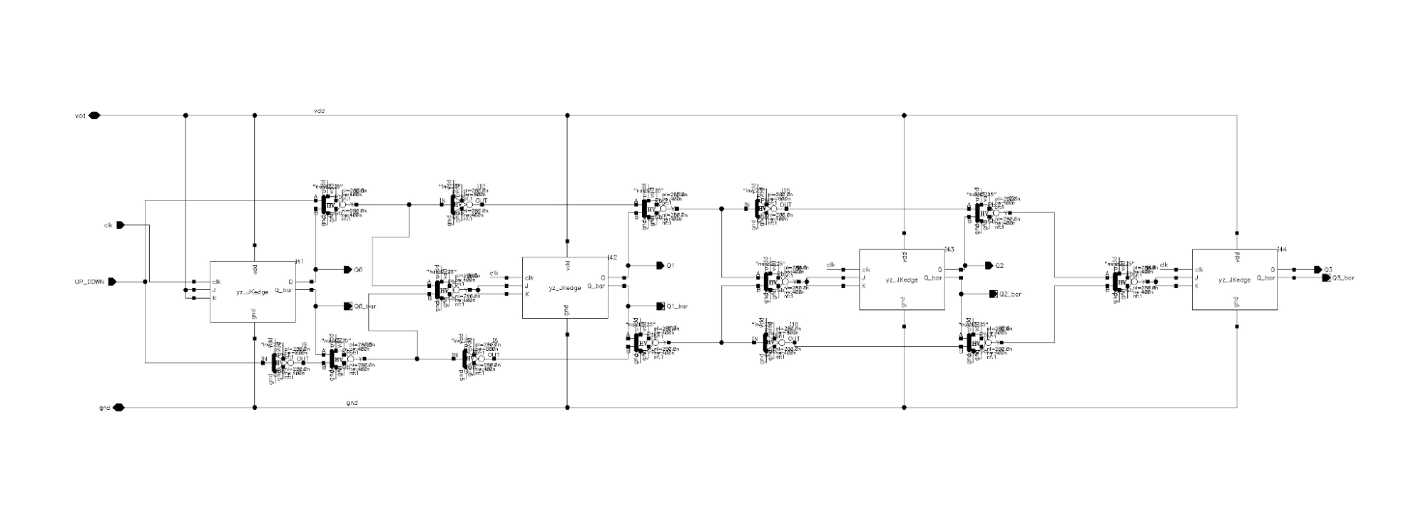
Figure. 4 The schematic of JK counter
Strong-Arm Comparator
In the Figure. 5, we use a strong-arm comparator to compare two voltages that come from the capacitor DAC array after assuming the next bit is 1. The comparator would verify whether this guess is correct or not. Apart from the schematic of the comparator, we also have dummy mosfets to prevent mismatch and make the whole comparator more stable.
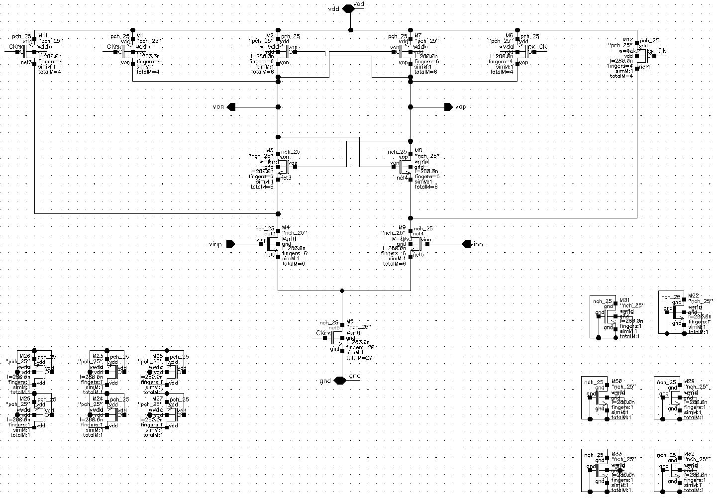
Figure. 5 Schematic of Comparator
10-bit Capacitor DAC & Switch
The Figure. 6 shows the unit switch design. Since driven capacitors would become larger and larger, the driven ability should also be bigger. Since the value of capacitor times 2 from the LSB to MSB. The driven ability should also increase according to this speed. So we choose to increase the number of unit switches 2 times with every bit increasing.
Figure. 6 The Unit Schematic Design of Single Switch
The Figure. 7 illustrates the half part of the capacitor DAC since our SAR ADC uses differential input. For each side, we have 10 bit Switches and 10 capacitors. The unit capacitor value is 22fF. We can calculate the minimum value requirement value of capacitor in the following method:
KT/C=Noise_power (Where K = 1.38064852e-23 T = 298)
Noise_power < quantization_noise_power
Quantization_noise_power= ((Vref/2^N))^2/12 (N=10)
The result shows the total capacitor should be larger than 8fF, which means our selection is reasonable.
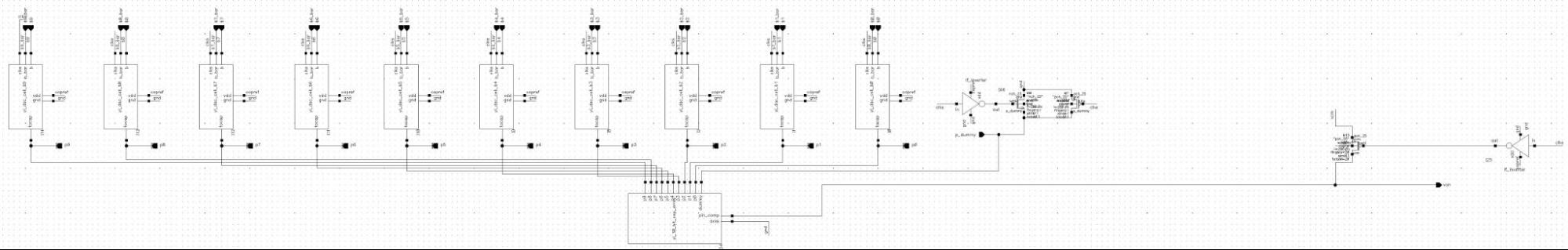
Figure. 7 Capacitor DAC
SAR Logic Block
Figure. 8 is the unit design of D-flip-flop used in the SAR logic block. Figure. 9 illustrates the schematic of the SAR logic block. The upper side is the result register to store the result value from the comparator. The bottom side is actually a 10-bit shifter to give the initial value for every bit. There is a delay line between them, which is used to give extra time to wait for the result from the comparator to compare two values. This delay line is a little risky so we give it 2 us delay(the comparator usually costs 500ps).
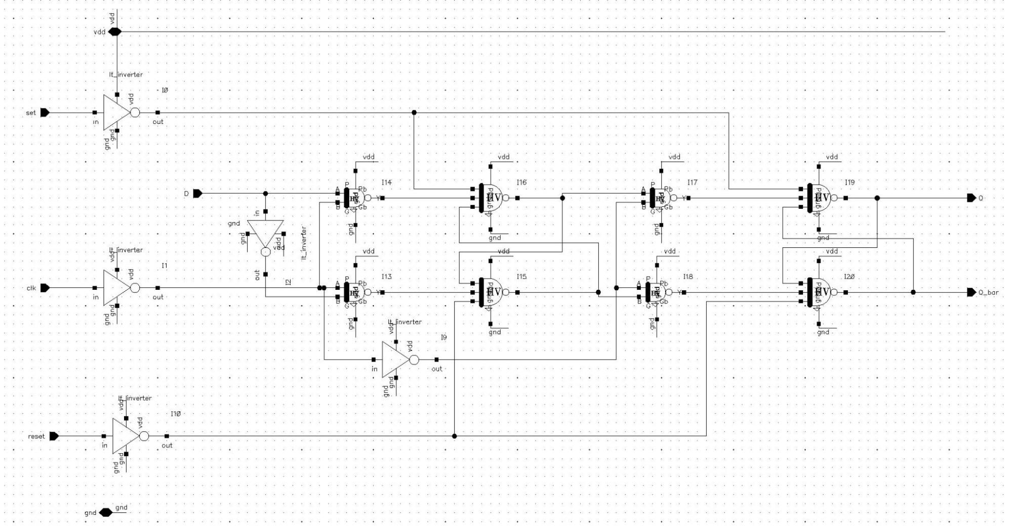
Figure. 8 Unit Dff in the SAR Logic Block
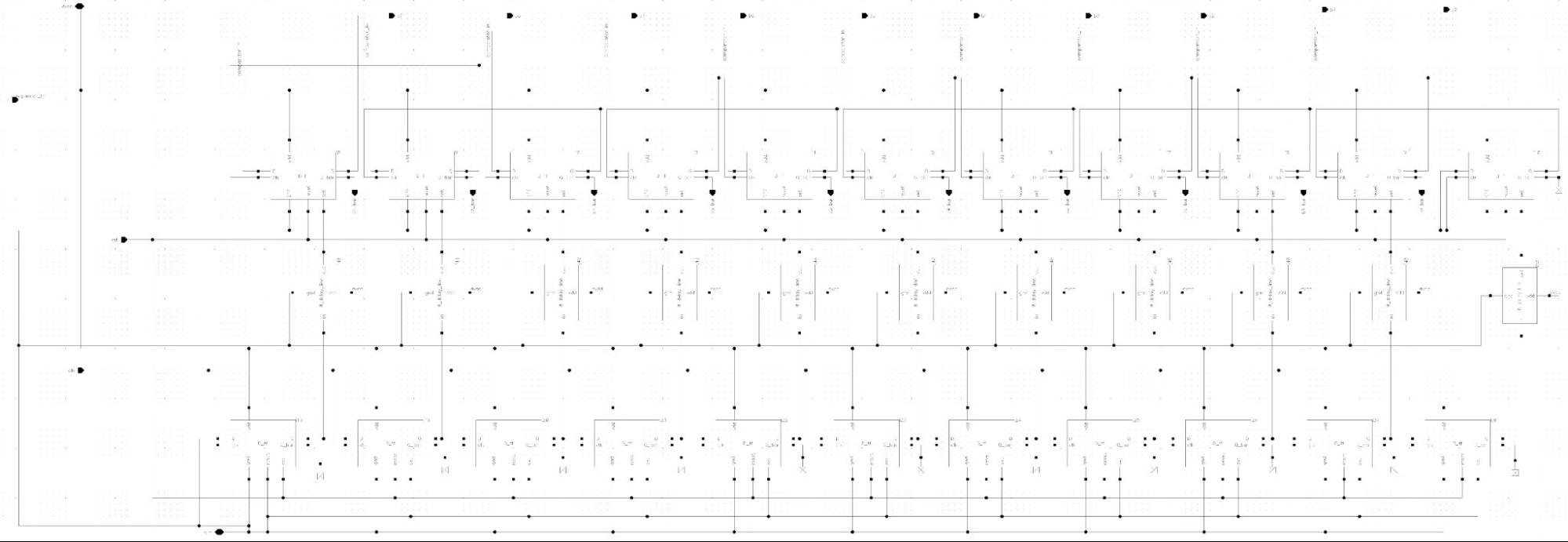
Figure. 9 Schematic of SAR Logic Block
10-bit R2R DAC
Our DAC adopts an R2R structure. After the digital signal enters the DAC, it is sampled by the input register at a sampling rate of 100k, and then the sampled signal is input to the input buffer. The 10 digit input digital signal controls 10 switches to control the input connection of the resistor array Vrefp or Vrefn. There is also an OTA at the output end of the resistor array as a buffer for the analog signal.
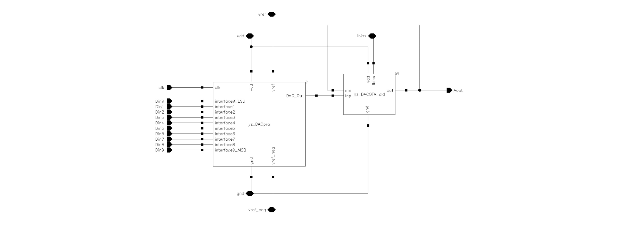
Figure. 10 The Top-level of 10 bits R2R DAC
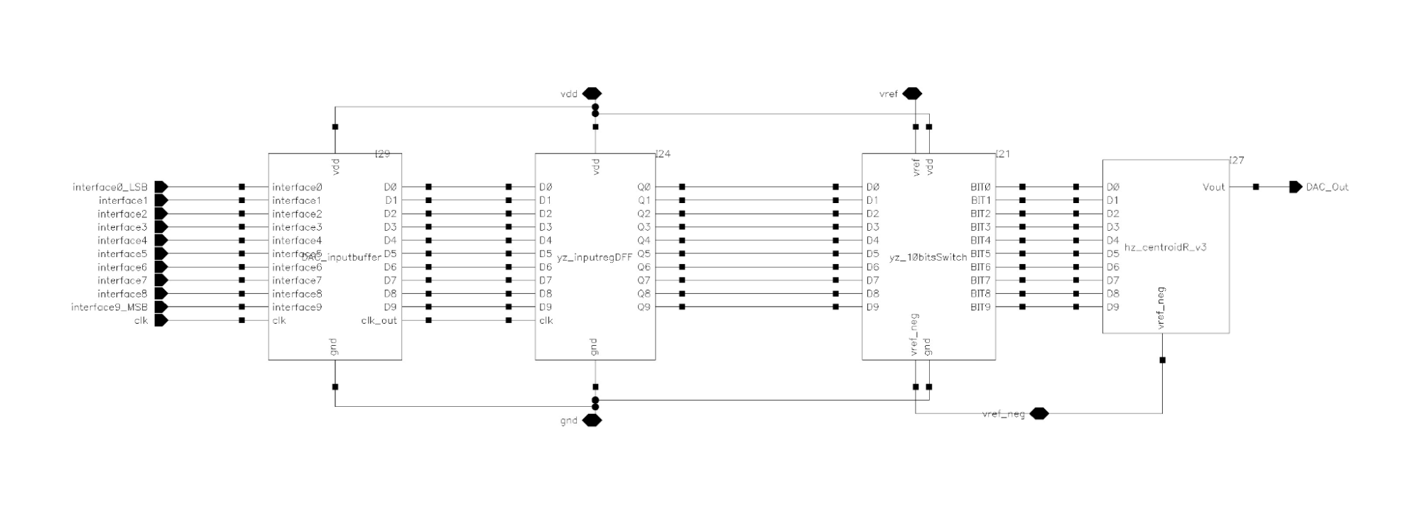
Figure. 11 The blocks of 10 bits R2R DAC
Input register
Using a simple Flip Flop to implement input register function with 100K samples/s sampling rate.
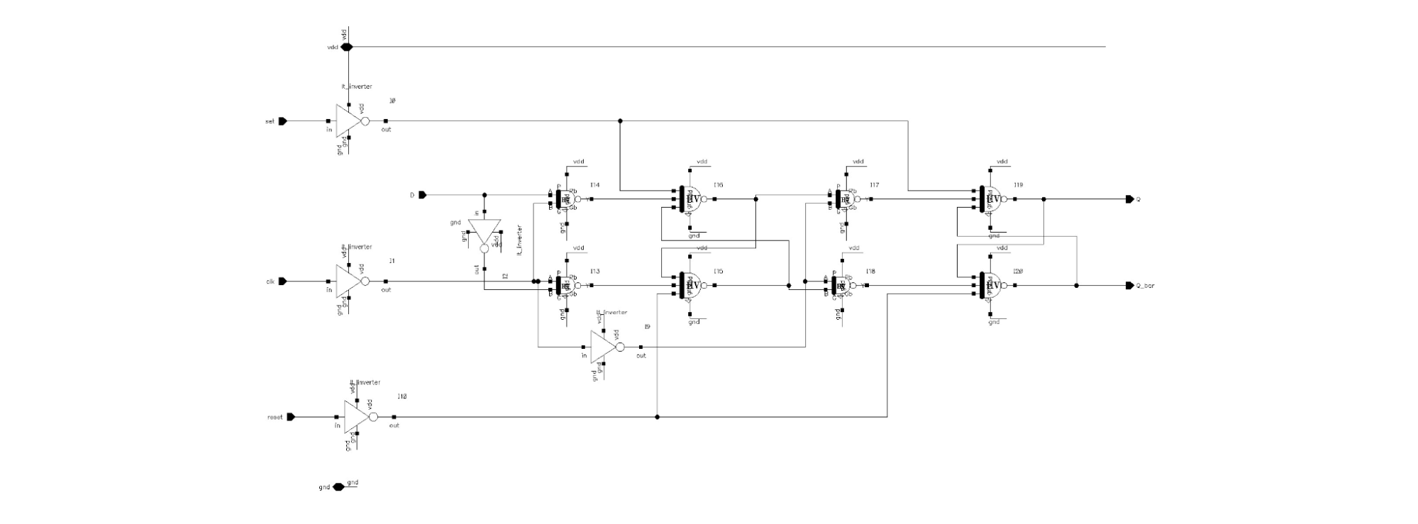
Figure. 12 The schematic of the DFF
Switch array
Because directly outputting the input voltage to the resistor array will result in different driving capabilities. We choose to use these input signals to control the switch connection vrefp or vrefn. At the same time, the switch is also controlled by the clock.
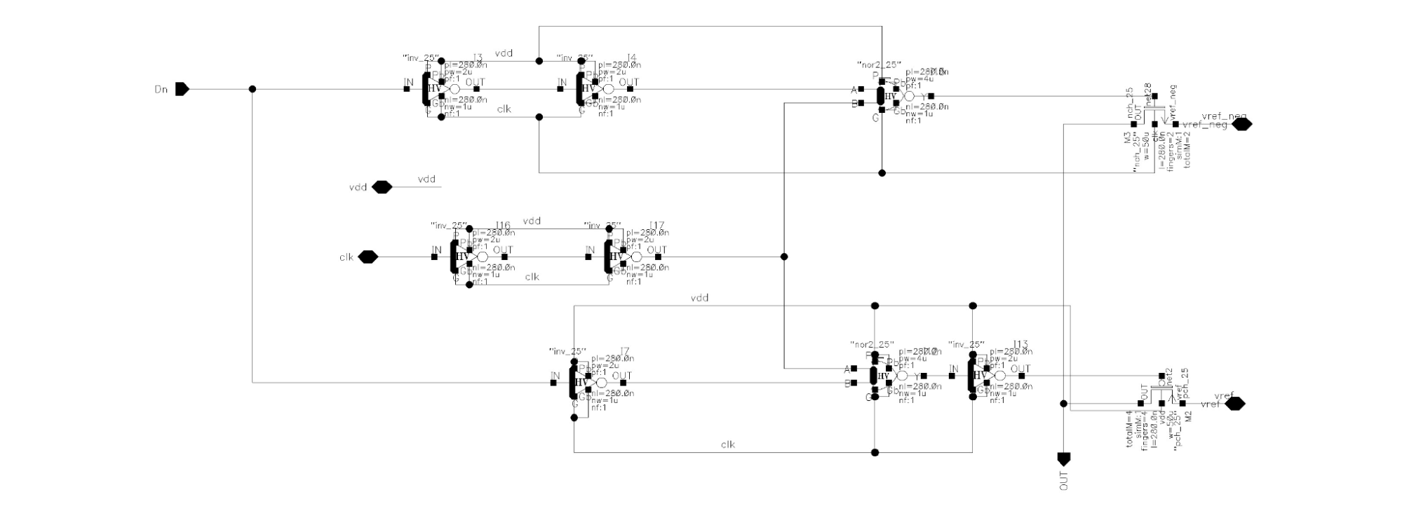
Figure. 13 The schematic of a unit switch
Resistor array
We choose resistors of 40k ohms and 80k ohms to achieve a resistor array. For a resistance of 40k ohms (40000 ohms), the thermal noise voltage is approximately 25.4 nanovolts. For a resistance of 80k ohms (80000 ohms), the thermal noise voltage is approximately 36.0 nanovolts, which is much lower than the voltage value of our LSB
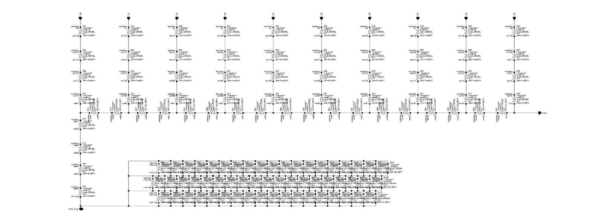
Figure. 14 The schematic of the Resistor array
OTA design
A second-order Miller compensated amplifier is an advanced design technique used to enhance the frequency response and stability of amplifiers, particularly operational amplifiers with high gain. This method employs two capacitors instead of one, as seen in traditional Miller compensation, introducing two poles in the amplifier design for improved frequency response control. The advantages of this approach include better stability across a wider frequency range, increased gain-bandwidth product without sacrificing stability, and reduced loss in phase margin. Second-order Miller compensation is especially beneficial in high-performance operational amplifiers, where precision and speed are crucial, and is often used in applications involving audio and video signal processing where wide bandwidth and high stability are required.
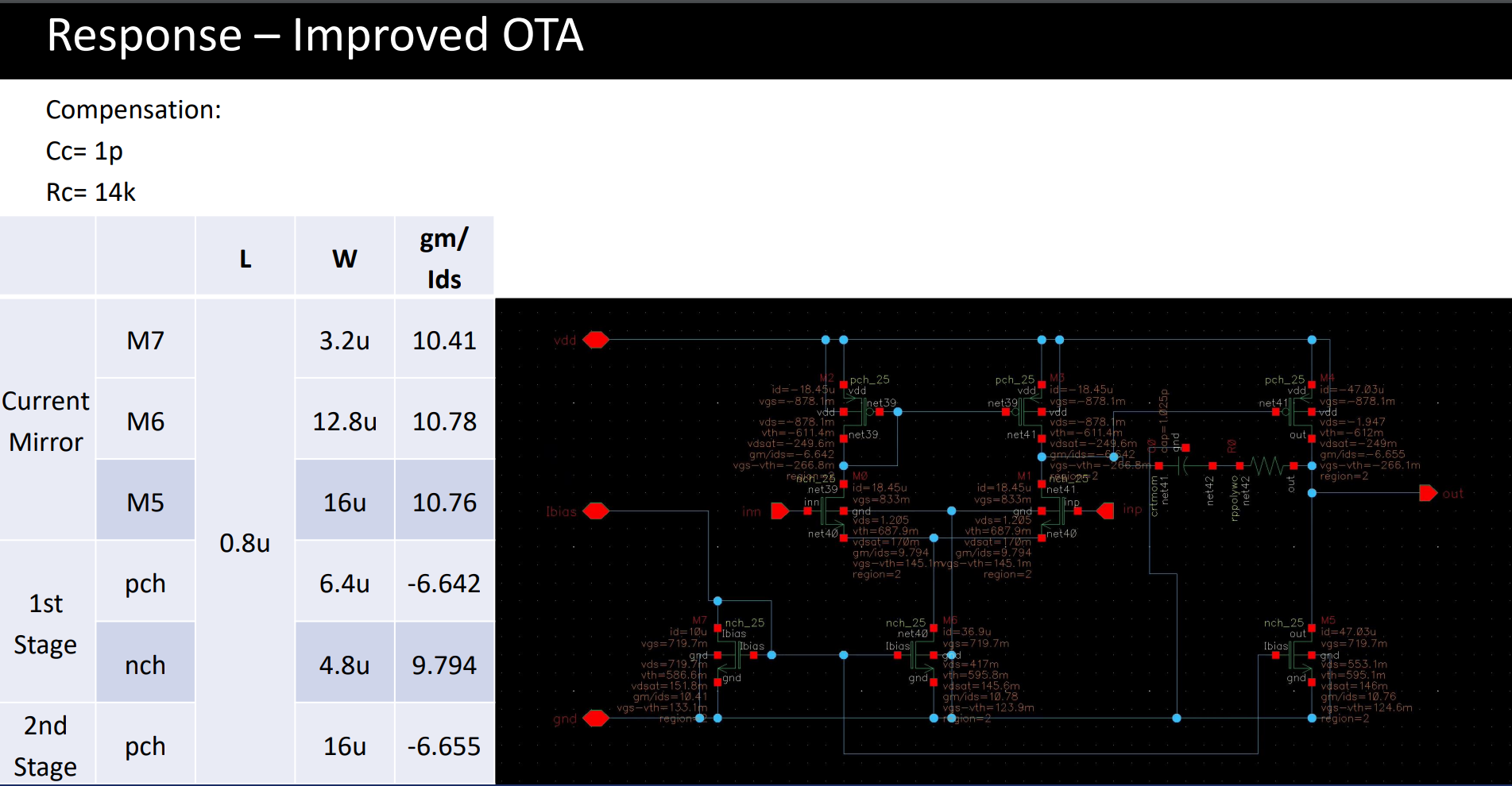
Figure. 15 The design of the output OTA