
Measurement Results
1. Technical test Purpose: Test whether the DAC chip can normally receive the input signal and convert the digital signal to analog signal output. Under the conditions of input voltage range (800mV to 1.8V) and sampling frequency 100KS/s, check the output waveform and frequency response of the DAC chip. Performance Testing Test the effective number of bits (ENOB) of the DAC chip. Test dynamic performance indicators: signal-to-noise ratio (SNR), signal to-noise-to-distortion ratio (SINAD), total harmonic distortion (THD), and spurious unrelated noise (SFDR).
Method: Use a digital signal generator to generate a single frequency sine wave signal (such as 100kHz), which will be transmitted as an input signal to the DAC chip. Connect the output of the signal generator to the digital input terminal of the DAC chip. Provide appropriate power supply voltage for the DAC chip and use a power supply to provide a stable power supply for the test PCB board. Connect the probe of the oscilloscope or spectrum analyzer to the analog output terminal of the DAC chip to measure the analog signal converted by DAC. Record the waveform, amplitude, frequency, harmonic, and stray components of the output signal displayed on the oscilloscope or spectrum analyzer. Calculate the ENOB, SNR, SINAD, and SFDR parameters of the DAC chip by analyzing the collected analog signal data
2. PCB test Purpose: Determine if the off-chip module is working properly and ensure that the PCB board at different temperatures will not cause any impact
Method:
1. Test the voltage of each node on the PCB to ensure it is within the normal operating range.
2. Check the output voltage stability of the power regulator.
3. Test the impedance matching of the signal transmission line on the PCB.
4. Use an oscilloscope or network analyzer to test the signal transmission characteristics on PCB.
5. Test the performance stability of DAC chips at different operating temperatures.
6. Measure the temperature rise of the PCB to ensure it is within the normal range.
3. Independent testing of each module
Input Register Module Test
a. Test whether the register module can receive input signals normally.
b. Check the performance of the module at different operating frequencies.
Switch module testing
a. Test the switching speed and reliability of the switch module.
b. Check the input and output impedance of the switch module.
R2R resistance string module testing
a. Test the linearity and matching of the resistance string.
b. Check the temperature coefficient of the resistance string.
OTA output buffer module testing
a. Test the gain and bandwidth of the OTA output buffer.
b. Check the input and output impedance matching of the output buffer.
c. Test the distortion and noise performance of the output buffer.
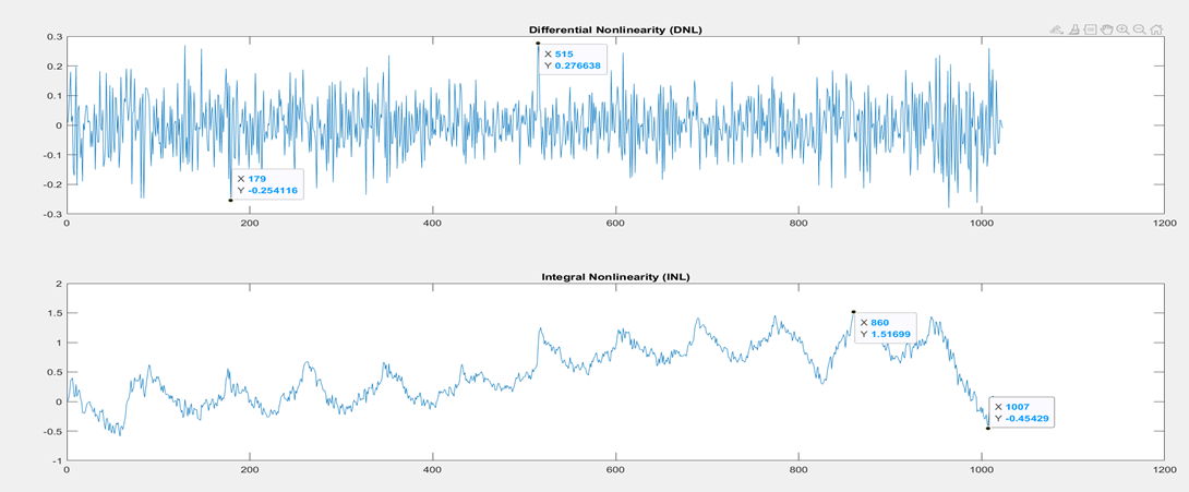
Figure 1. The plot of DNL/INL
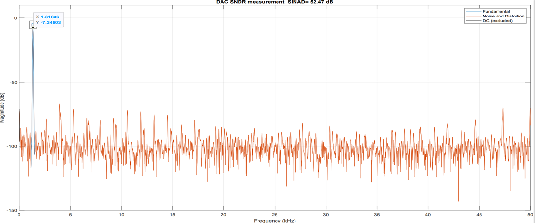
Figure 2. The FFT of the output signal with 1.318kHz input sine wave
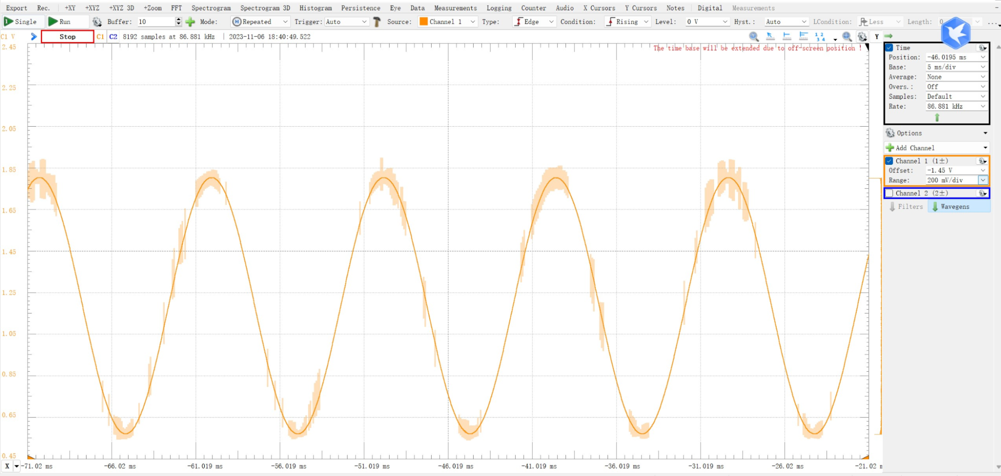
Figure 3. The output signal with 1.318kHz input sine wave
ADC Measurements:
The ADC is 10-bit 100K samples per second. The voltage supply is 2.5V. We use the analog discovery 2 (AD2) to connect to the chip on the breadboard. The analog discovery would provide differential input signal, common-mode voltage and sample the result from 10 bit at 100KHz. However, since the AD2 cannot provide 2.2MHz clock frequency accurately. We have to use two waveform generators to give 2.2Mhz clock frequency and 100KHz clock frequency to the chip. The 2.5V supply comes from the DC power supply. In this setup, we measure the ADC results as following:
After collecting the data from AD2 and transforming them back to decimal format. We get the output signal spectrum as you can see in Figure. 4. There are still several skirts on the Figure, which indicates that spectrum leakage happens. This is because we cannot make every signal synchronized. The clock frequency crystal oscillator in the AD2 supplies would have a little difference with the clock frequency crystal oscillator in the waveform generators supplies. This difference would make a huge mistake for the ADC performance measurement. However, even with this spectrum leakage, we can still get a 7.78 bits ENOB. In addition, the noise voltage in our PCB is about 2mV while our ADC LSB voltage is 2.44mV. This is the second disturbance for ADC measurement.
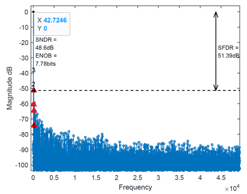
Figure. 4 The Full Range output signal Spectrum with 42.7246Hz input frequency
The spectrum leakage would decrease the result of ENOB and this distortion becomes even bigger when it comes to higher frequency. In this situation, we have to use the window function to recover the original ENOB. The Figure. 5 is the result of ENOB vs frequency. The former two points are not bad enough to use the window function to recover ENOB. But we have to use the window function for other points. As you can see, the ENOB oscillates around 7.5 bits.
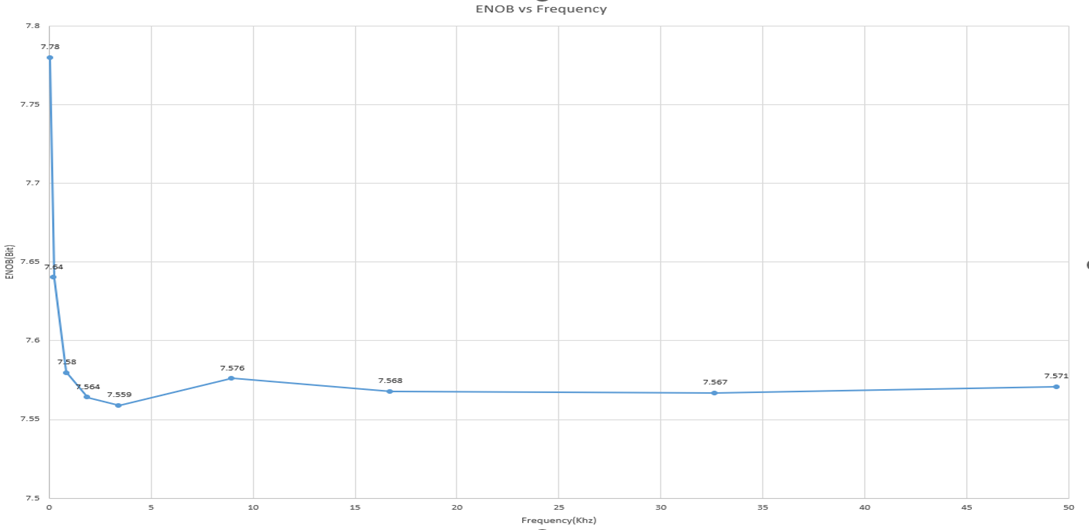
Figure. 5 The Full Range Result of ENOB vs Frequency
The Figure. 6 show the result of INL and DNL, we use a very slow sine wave input and collect the result. And we can use matlab to generate statistical results for every ADC step. The spectrum leakage also happens in this measurement, which means we can not sample complete cycle results. This would decrease the result of DNL and INL. Eventually, we get the -0.99LSB-0.66LSB DNL and ±2.0LSB INL.
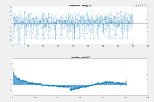
Figure. 6 The Result of INL and DNL for SAR ADC