
SYSTEM OVERVIEW
WWVB signal has two modulation schemes: PWM and PM. In this project, the chip reads the signal under pulse width modulation scheme. Although the phase modulation scheme allows faster and more accurate synchronization along with features like hamming code and message frames, the design is much more complex and much less suited within the time scope. The PWM works in ternary symbols: '0', '1', 'M', where 'M' bit means a 'marker'. Fig. 1 presents the PWM symbols:
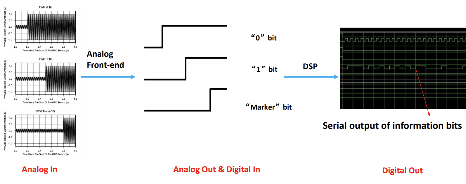
Fig. 1: PWM symbols, the duty cycle of the PWM symbol determines the ternary bit
The WWVB signal is continuously transmitted, and the broadcast time frame is shown in Table 1 (PWM format in black):
Table 1: WWVB one-minute time frame (PWM format in black)
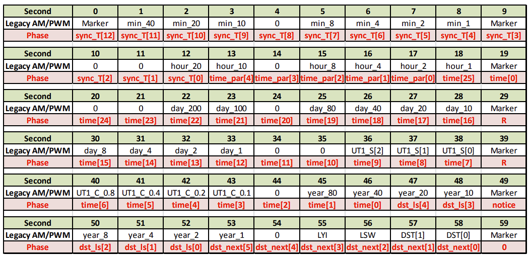
The significance of markers comes from two points:
1. It creates a rough frame that allows some error detection in terms of reception duty cycle accuracy.
2. The beginning and the end of a frame being markers indicates the beginning and the end of a full minute.
The second fact is crucial. It means that the start of a minute can be observed if two consecutive markers appear during the reception. The decoding process relies on this observation.
With a better understanding of the input signal, we can now take a look at our system. The system consists of our chip's analog front-end, digital back-end, and the microcontroller.
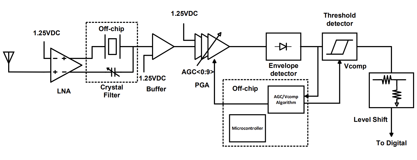
Fig. 2: Analog front-end block diagram
The WWVB signal will first be received on a ferrite rod antenna, go through an LNA, pass through a tuned crystal filter to reject noise. Then the buffer amplifier presents certain loading to the crystal and amplifies the signal. The programmable gain amplifier (PGA) is responsible to bring the received signal level to a point such that low or high binary voltage can be determined. Being programmable provides the ability to adjust the amount of gain under various input signal strength (scenarios like different location, different time, etc.). The PGA series has very high gain under high AGC level (gain setting) because the input signal received at New York is extremely small: WWVB Coverage Area
The envelope detector acts as a rectifier, only keeping the "envelope" of the signal and removing the carrier sinusoid by having possessing large time constant. The threshold detector is a schmitt trigger comparator that converts the envelop detector output into clean, binary digital output. Since, in this technology node, analog supply is 2.5V and digital supply is 1.0V, a simple voltage divider is used to convert 2.5V logic level to 1.0V digital logic level, as the signal is extremely low-speed and rise/fall time are non-critical. An off-chip AGC algorithm is implemented using a microcontroller. The microcontroller utilizes an ADC channel to read the envelope detector output, interpret it, then sends AGC bits to the chip, and also configures an appropriate comparator reference voltage to the threshold detector via a DAC channel.
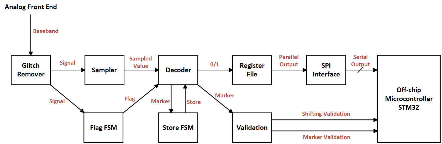
Fig. 3: Digital back-end block diagram
The level-shifted digital signal is then fed into the digital back-end. First, we implemented a glitch remover which can remove the glitches that the analog part cannot process. Then, the signal without any glitches will be sent to the sampler which is a counter. Because of the PWM nature of the signal, the beginning and the end of a symbol needs to be determined. The Flag FSM detects the negative edge of the input signal, indicating the beginning of a symbol, and detects the positive edge to start counting. The sampler will count how many clock cycles of the signal staying high, and the sampler will reset to zero when the signal switches from high to low. The sampling clock frequency, which is the digital system clock frequency, is 10kHz. The decoder block identifies the symbol from the sampler output by comparing the thresholds among '0', '1', and 'Marker'. The Store FSM will monitor the decoder output to see when the two consecutive markers appear. If you can please see the format frame above (Table 1), two consecutive markers indicate the start of a new minute (second 59 and second 0). The register file is a place to hold all the 0 and 1 bits. This register file will be written only when the store signal is high. Once all of the bits have been sampled and stored, a signal called micro_enable will be sent to the off-chip microcontroller, enabling SPI communication. Error detection method is also implemented on-chip. This is done by tracking the marker's quantity and position within the frame. These two validation bits are also sent to the microcontroller after micro_enable is pulled high.
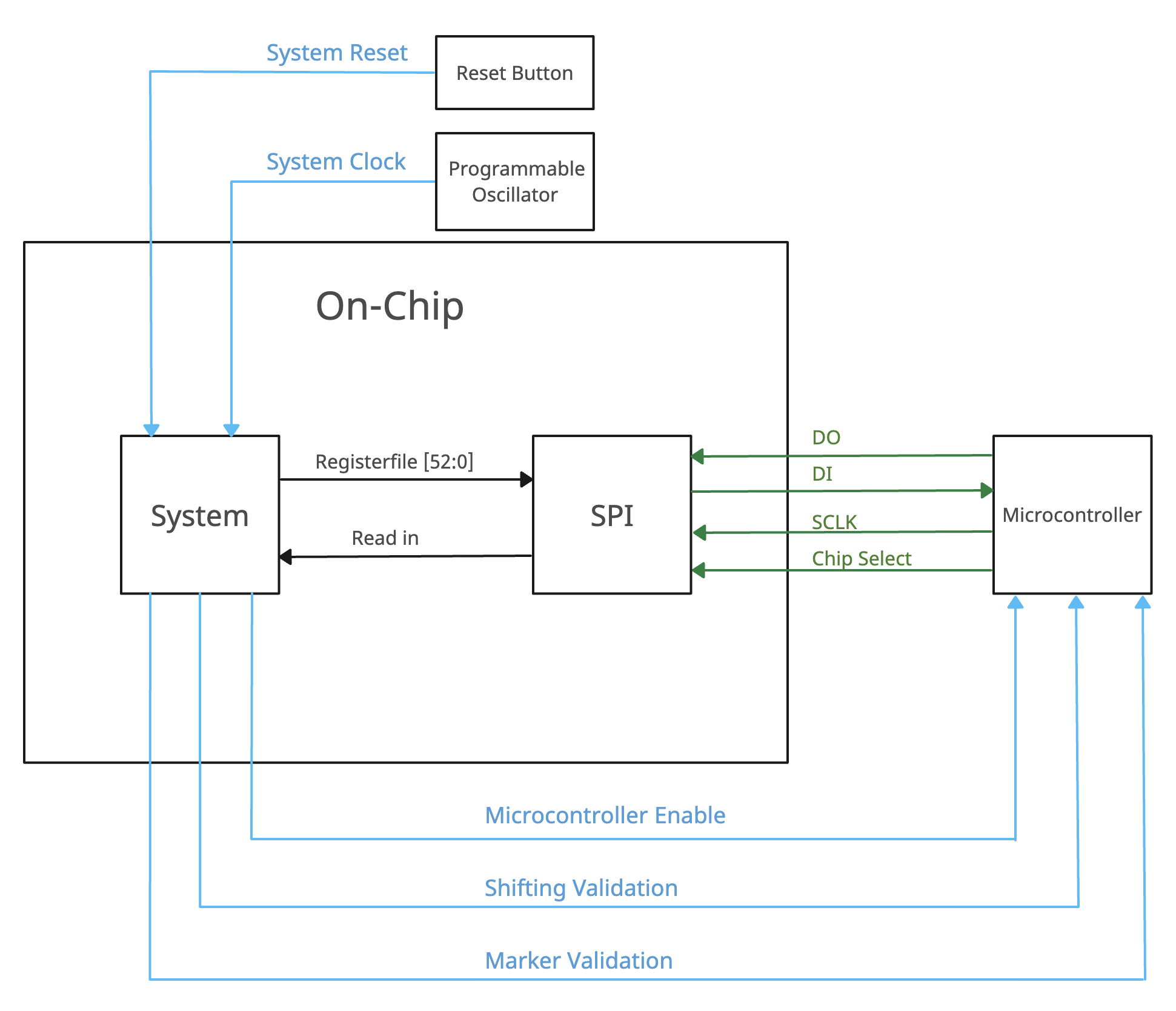
Fig. 4: On-chip and off-chip communication
As we mentioned before, the digital part has the system module and SPI module. When the register file has been filled up with 53 information bits, there is no way to do a parallel output to the off-chip microcontroller since we do not have enough pinouts on the padframe. Consequently, we implemented a SPI module to do the serial output. When the register file has been filled up, the system will send out a signal called micro_enable to the microcontroller. The microcontroller detects the micro_enable and recognizes that the data is ready. Then it initiates the SPI data exchange by pulling the chip select line low. The idle state of the clock line is low. The clock starts toggling after the chip select is low. The SPI data is read on the positive edge of the clock, and shifted on the negative edge.