
CIRCUIT DESIGN
ANALOG PART SCHEMATIC
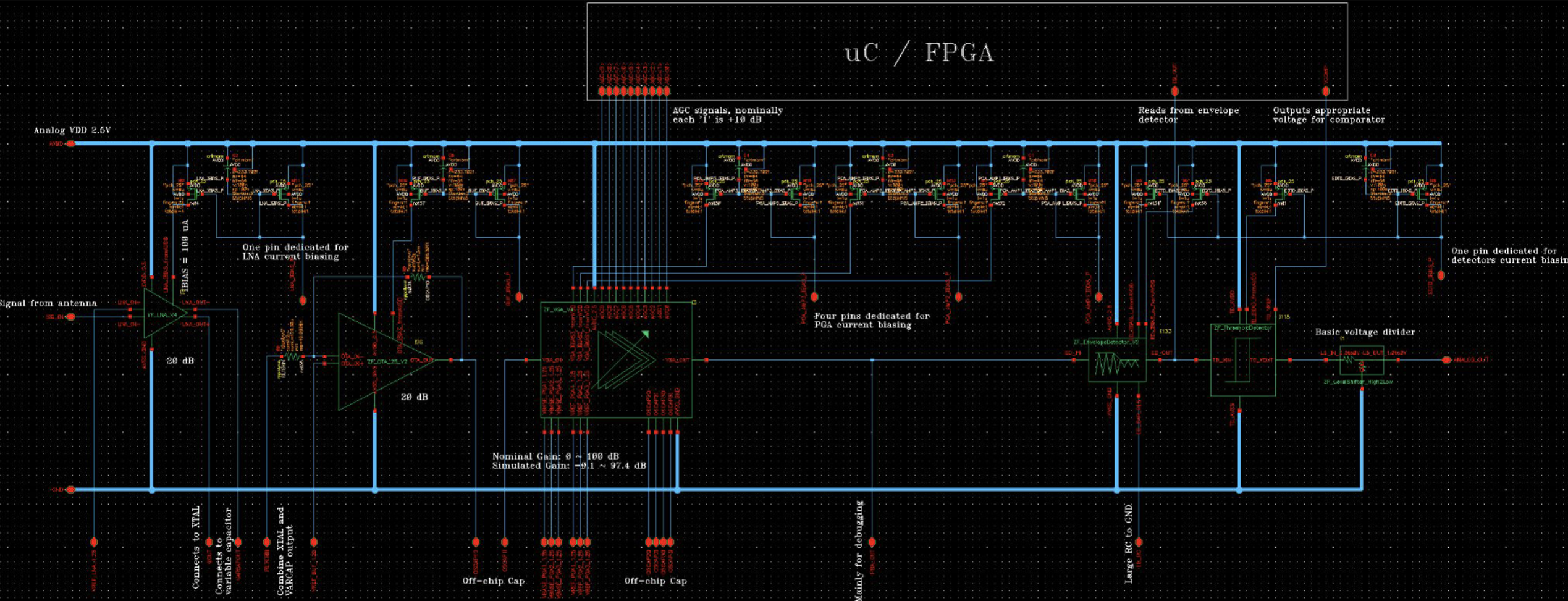
The AC signal coming from the antenna will first be DC biased off-chip, and then enters into the chip to the LNA. All nets that are connected to pads have gates with guard rings for DRC.
ANTENNA
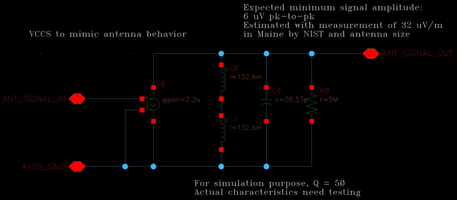
Fig. 1: Antenna lumped model
We use the ferrite rod antenna as the first "block" in the signal chain. The antenna was bought on Amazon and was the only compact-sized 60kHz antenna available to us. The antenna is slightly fine-tuned with a parallel 1.6nF capacitor. The resulting bandwidth is around 1kHz, center frequency at 67.76kHz, and the quality factor is 52.3.
LOW-NOISE AMPLIFIER
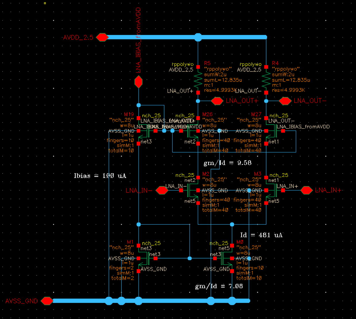
Fig. 2: Low-noise amplifier schematic
LNA can amplify the signal without introducing much noise. We designed the LNA to convert the single-ended input to differential output to drive the crystal and the phasing capacitor. The LNA utilizes cascode devices to suppress the miller effect of the Cgd, yield higher gain, and pose less capacitive load on the antenna. The bias current is 100uA, tail current is 481uA, and the gm/id is about 10. With 5kOhm resistor load, the gain is about 10 times or 20dB.
From noise calculation and simulation, the white noise component is about 2.5nV/sqrt(Hz). However, since the carrier frequency is 60kHz, the frequency band of interest includes flicker noise. The simulated noise is 3.7nV/sqrt(Hz) at 60kHz.
OFF-CHIP CRYSTAL FILTER
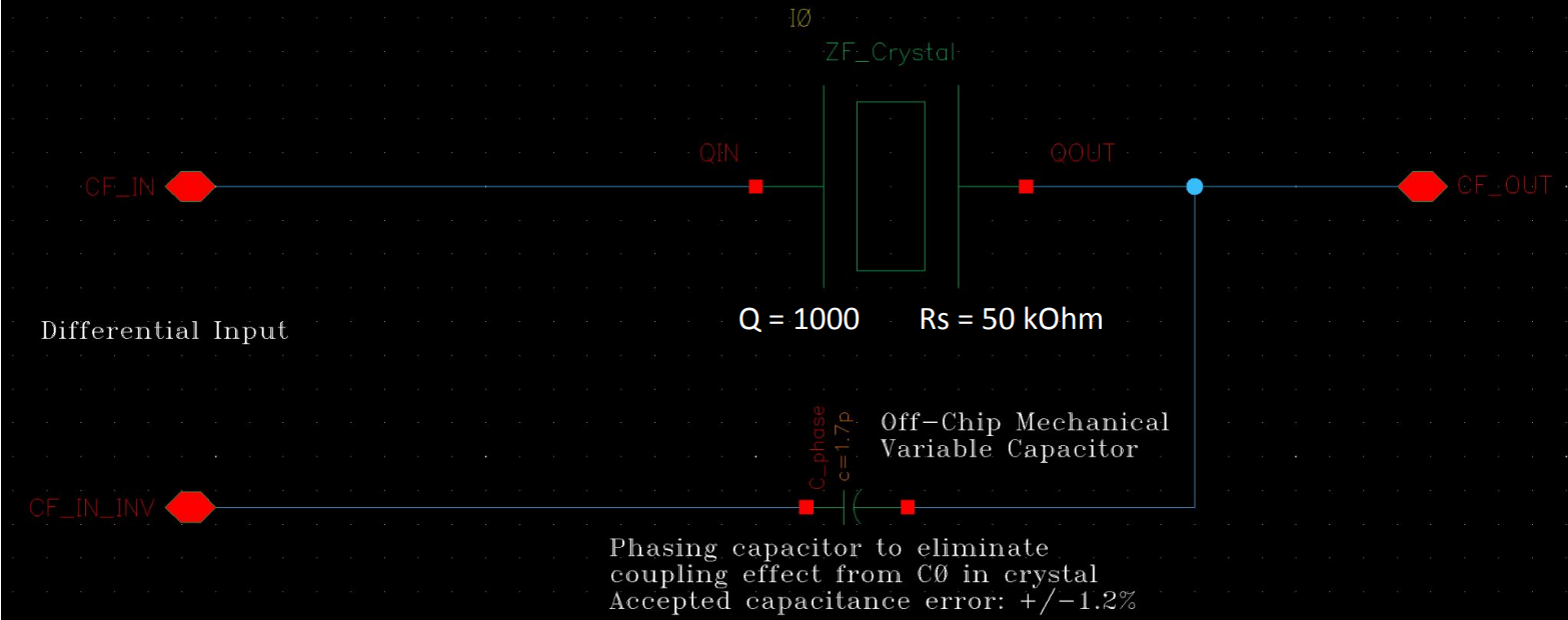
Fig. 3: Crystal filter schematic, the noted values of the crystal were estimations before measurement
The off-chip crystal filter is a bandpass filter. The center frequency of the crystal should be at 60kHz. The crystal has an extremely large quality factor such that the filter will have very narrow bandwidth, rejecting any blocker signals outside of the band. However, the out-of-band rejection performance is deteriorated due to the presence of parallel capacitance C0 in the model which provides a bypass for the signal around the signal. Therefore, a trimmer phasing capacitor is connected to the other end of the differential output which attempts to compensate the effect of C0.
OTA
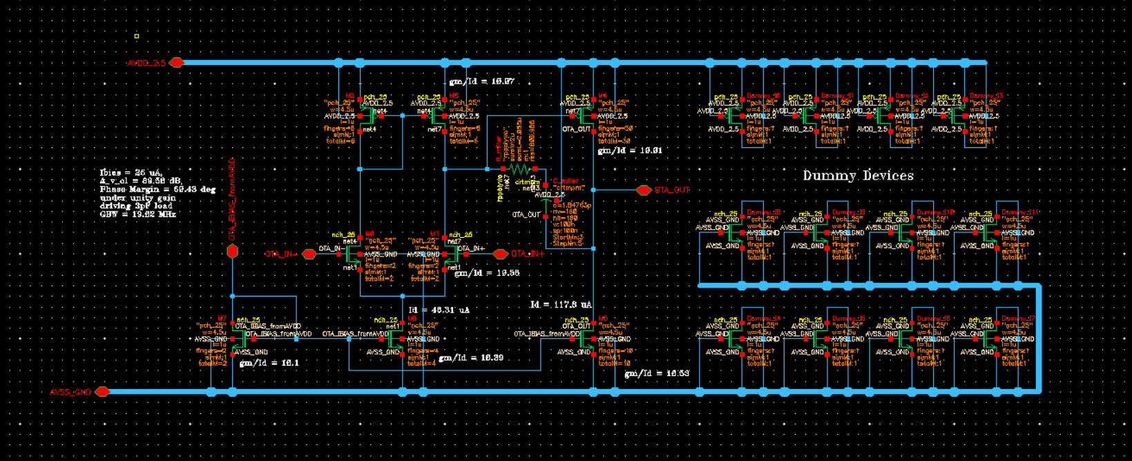
Fig. 4: OTA schematic
The OTA is used frequently in the rest of the signal chain. The structure is a simple two-stage miller compensated single-ended OTA. The OTA uses a bias current of 25uA. The gm/id selected for the devices is around 10. The open-loop gain of the OTA is 89.58dB. The phase margin is around 60 degree under unity gain feedback, driving a 3pF load. The gain-bandwidth product is 19.02MHz. The OTA is well-compensated when used in the rest of the blocks as they all incorporate some feedback factor lower than unity (except envelope detector buffer which is in unity gain feedback, but it is also sufficient).
PROGRAMMABLE GAIN AMPLIFIER
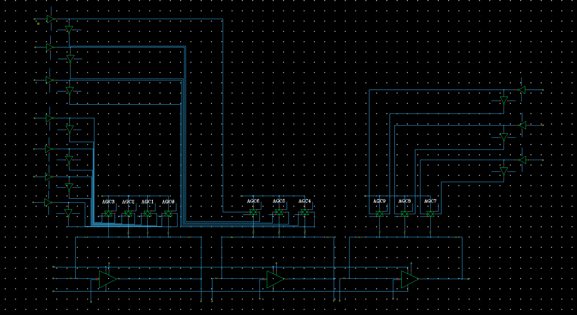
Fig. 5: Programmable gain amplifier schematic
The programmable gain amplifier is used to further amplify the signal until a reasonable level is reached. The necessity of amplifier being programmable comes from the variation in signal strength when synchronizing at different location and different time of the day. The amplifier stages utilize T-shaped feedback, allowing resistors with less values to be used while still achieving high gain. The variable gain is implemented by digitally switching the "T bottom" resistance with transmission gates. 10dB gain steps are realized by turning individual transmission gates on in a specific designed order. There are 10 gain steps available, each corresponds to a 10dB gain increase and combines to 100dB gain in total if all AGC bits are enabled. Gain steps will be applied to the first stage first because of supply feedback and PSRR issues.
ENVELOPE DETECTOR
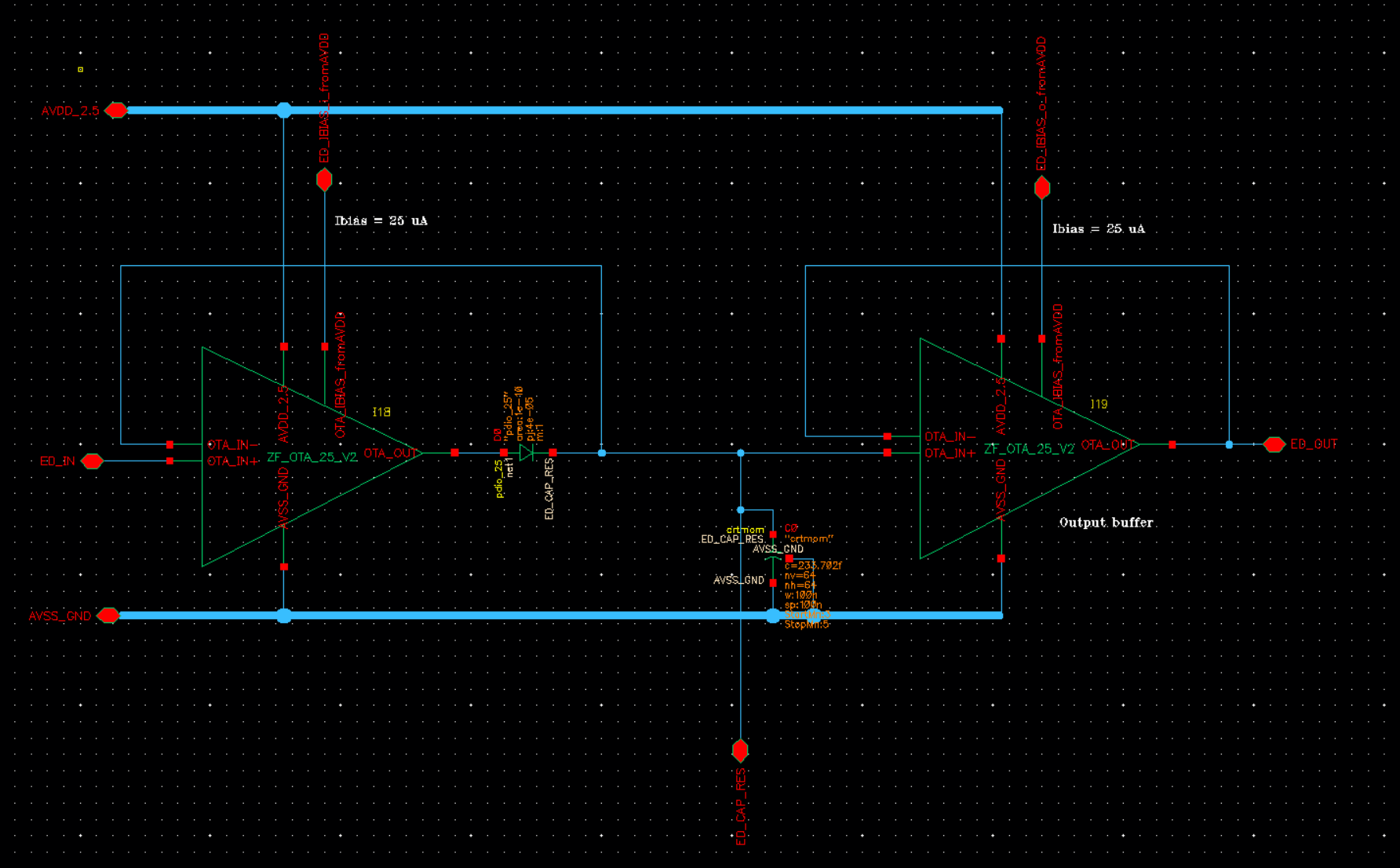
Fig. 6: Envelope detector schematic
The envelope detector removes the relatively high-frequency carrier and only leaves with the "envelope" of the input signal. A common rectifying circuit is a diode followed by a large R and C shunt to ground. However, the diode would cause a relatively fixed amount of forward voltage drop for all input signal levels. By introducing OTA and feedback, the diode output node is forced to be close to the input as long as the input is one forward voltage less than the supply voltage. A buffer is used to isolate between the diode output node and the threshold detector input.
THRESHOLD DETECTOR & LEVEL SHIFTER
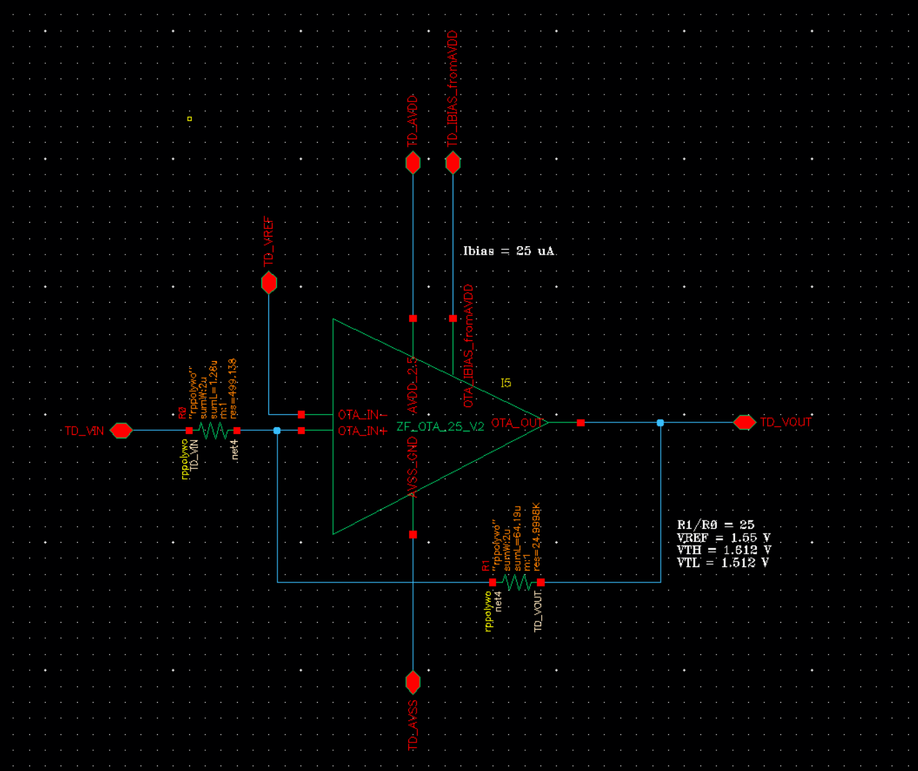
Fig. 7: Threshold detector schematic
The threshold detector is a schmitt trigger, which is an OTA in positive feedback. The threshold detector converts the analog envelope detector output into digital output under an appropriate comparator reference voltage. Because the digital part of our chip uses 1V devices, the 2.5V digital signal from schmitt trigger needs to be level-shifted down to 1V. This is easily achieved with a simple voltage divider since the speed of our signal is very low (1 bit per second) and the loading is rather small.
AUTOMATIC GAIN CONTROL
The automatic gain control is implemented on the microcontroller. Initially the AGC level is 0, corresponding to no gain in the PGA. In the beginning of the synchronization, the envelope detector output is monitored. The microcontroller samples the output in 2 second periods, and determines the maximum and minimum values during the period. If the maximum voltage isn't high enough, the AGC will increase the gain by adding one 10dB gain step. This is repeated until the threshold is reached or triggered by high noise level/oscillation due to high gain coupling (which yields garbage at output, of course). Because the actual crystal resonance frequency is at 59.996kHz, the output rise and fall transient response envelope exhibits slightly underdamped oscillatory behavior. As a result, in order to avoid glitches at the digital output, the comparator voltage should be lower than the Vmax - Vmin while trying to preserve an accurate duty cycle of the digital output signal:
AGC level 0 ~ 3: Vcomp = Vmin + (Vmax - Vmin) / (3 * A) where A is an empirical constant around 1 that depends on the AGC level
AGC level 4: Vcomp = Vmin + (Vmax - Vmin) * 1.01 / 2
AGC level 5: Vcomp = Vmax - (Vmax - Vmin) * 1.8 / 5
Only when the AGC level is determined, the microcontroller will notice the chip via the "SYNC" signal, pulling the line high for 2 seconds then pulling it down.
DIGITAL PART
We used the digital flow scripts provided by Ray Xu to generate the layout for the digital part using Cadence Genus and Innovus. The design steps include: 1. System Definition; 2. Architectural Design; 3. RTL Design; 4. Behavioral Simulation; 5. Logic Synthesis; 6. Post-Synthesis Simulation; 7. Place and Route; 8. Post-PNR Simulation; 9. AMS Simulation with Analog Part. The digital system and SPI functionalities were verified using Verilog testbenches and AMS simulations in Cadence Virtuoso (combined with the analog part).
The simulations shown below were all post-PNR simulations.
GLITCH REMOVER
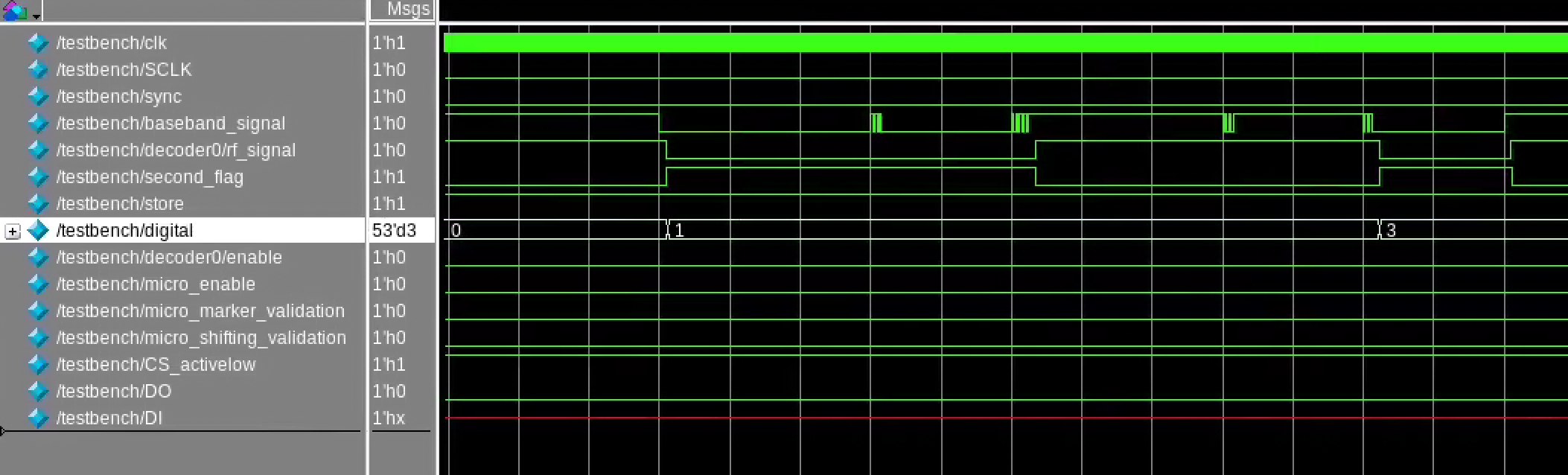
Fig. 8: Glitch remover module simulation
The baseband_signal is the output signal from analog front-end. The rf_signal is the glitch remover output. The signal received and the signal coming in need to be different for a certain time, or the rf_signal will not change to the new value.
STORE FSM
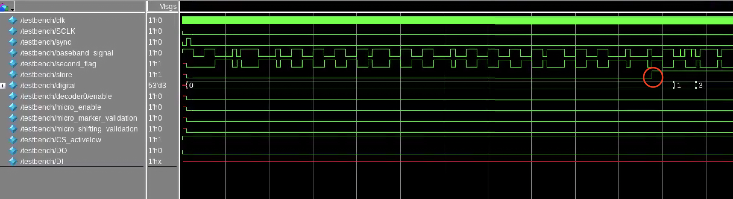
Fig. 9: Store FSM simulation
The store signal is used to control the decoder module to start storing bits into the register file. It will be high only after two consecutive markers are seen. If we look at the beginning of this simulation, two markers that are close but not consecutive are not considered as the beginning of a minute and thus do not trigger the Store FSM.
POST PNR SIMULATION OF DIGITAL DESIGN
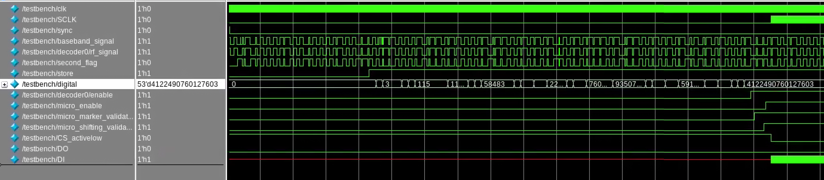
Fig. 10: Full post-PNR simulation
Post PNR can bring more compelling results for whether the design will be functional after tape-out. The baseband_signal is a test case for the whole digital processing chain.
SPI COMMUNICATION
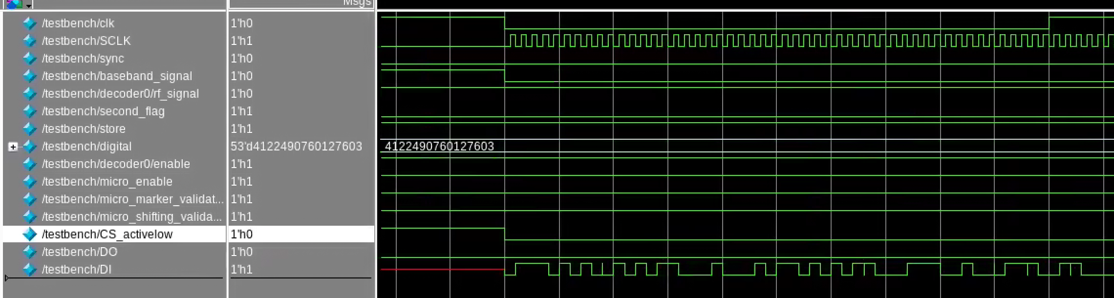
Fig. 11: SPI module simulation
The SPI interface is in receiving master only configuration. The implemented SPI mode is 0, which means the CPOL is 0 and CPHA is 0. The SPI internal buffer size is 64 bits width.