
IC LAYOUT
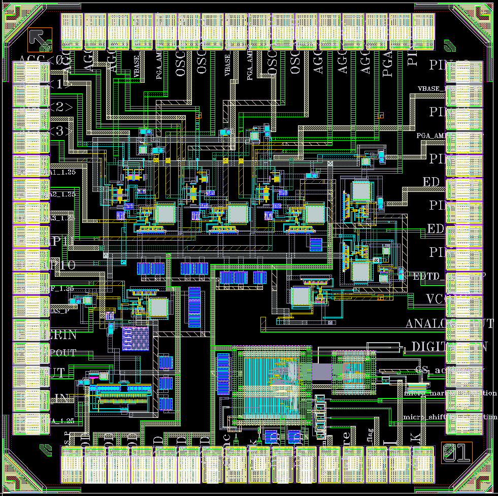
Fig. 1: WWVB Receiver Chip layout without dummy filling
LOW-NOISE AMPLIFIER
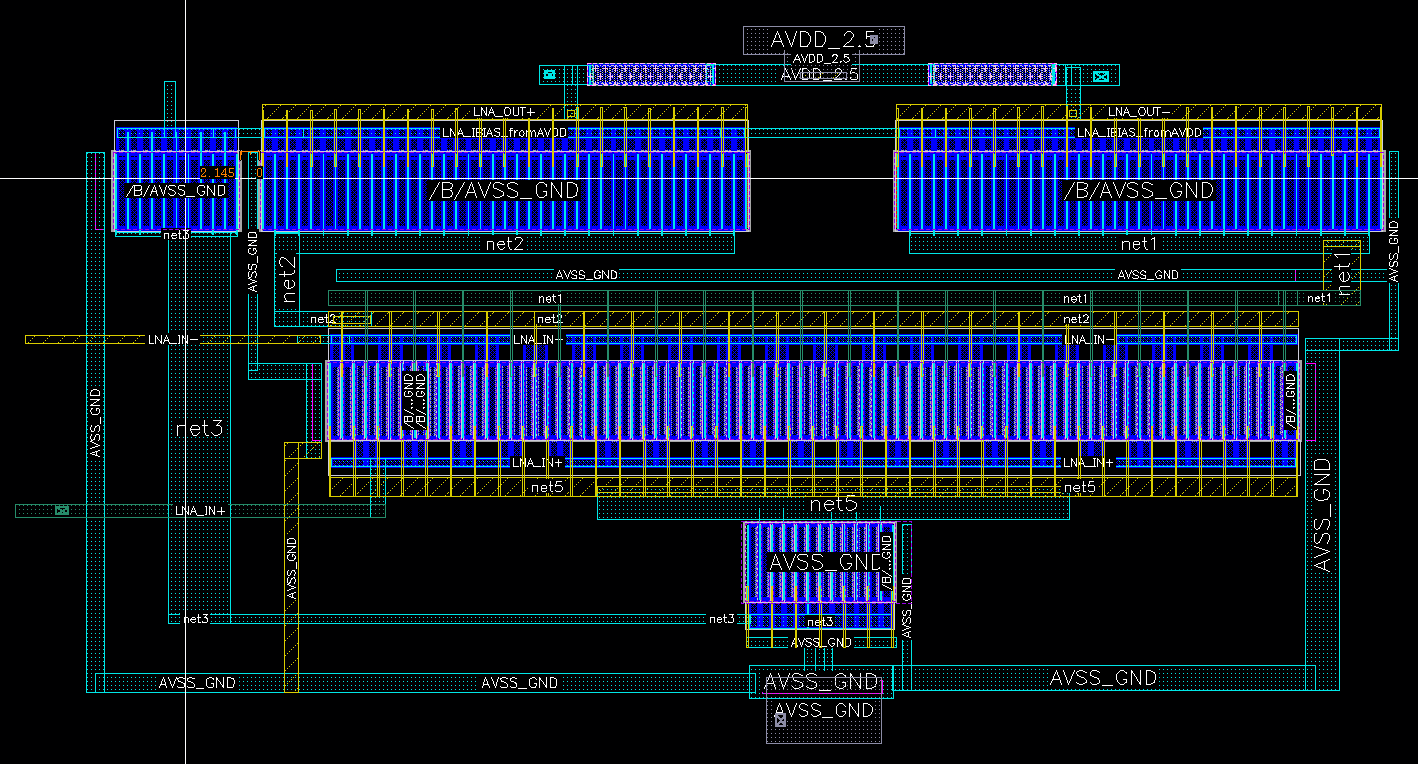
Fig. 2: Low-noise amplifer layout
The LNA layout utilizes interdigitated connection for the input pair. Bottom tail device and current mirror are combined for matching.
OTA
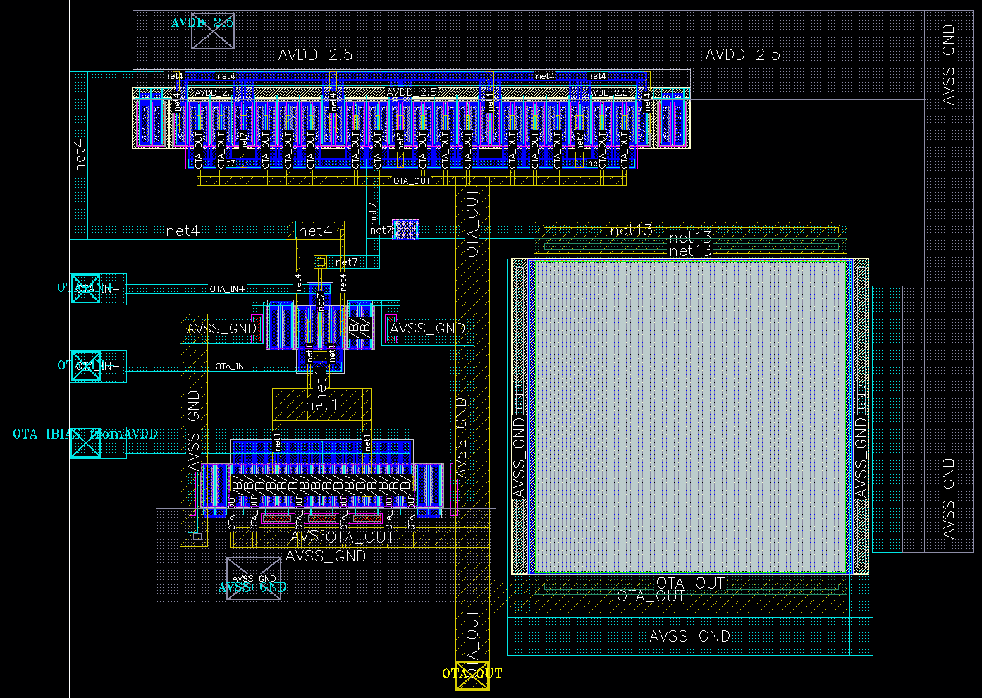
Fig. 3: OTA layout
The top row and bottom row are all interdigitated to decrease device variation in horizontal direction. Each row has dummy devices on the sides. The large rectangle on the right side is the miller compensation MOM cap.
PROGRAMMABLE GAIN AMPLIFIER
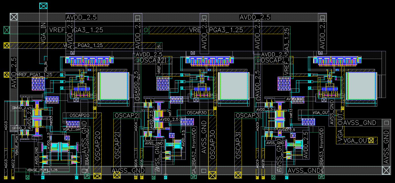
Fig. 4: Programmable gain amplifier layout
The programmable gain amplifier has three OTA circuits in cascade. Power rails use higher level metal. Each stage's output is at bottom.
ENVELOPE DETECTOR
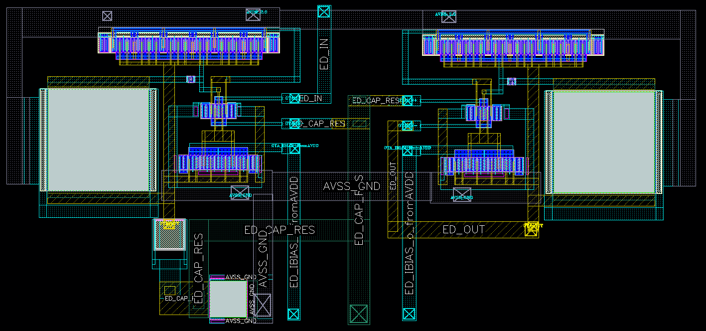
Fig. 5: Envelope detector layout
The envelope detector has two OTAs. The rectifying diode is constructed using (this needs to be determined and written). The required large RC are provided off-chip.
THRESHOLD DETECTOR
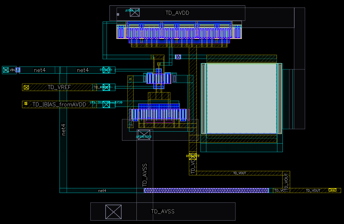
Fig. 6: Threshold detector layout
The threshold detector is a schmitt trigger, an OTA with positive feedback resistors.
DIGITAL DECODER
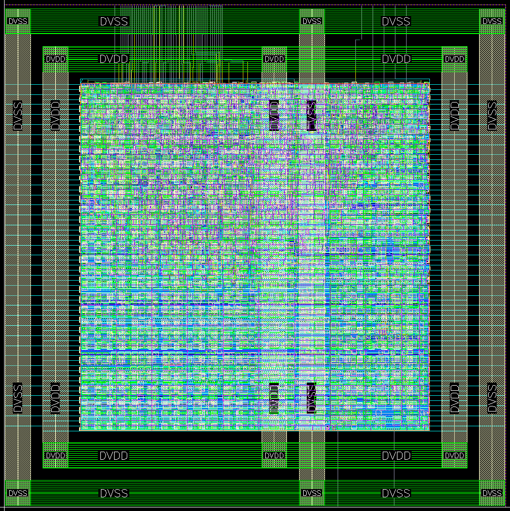
Fig. 7: Digital decoder Auto place-n-route layout
The digital part is achieved by RTL implementations of each block. We used Cadence Genus and Innovus to generate the layout, and then port back to Cadence Virtuoso to integrate with the analog part. We used the reports provided by Innovus to do the static timing analysis and power analysis.
The first one is the system module, decoder. It is 180 * 180 micrometers. As we can see, the thin gray wires at the top left are the parallel decoder outputs. The few wires at the top right are the digital control signals.
SPI
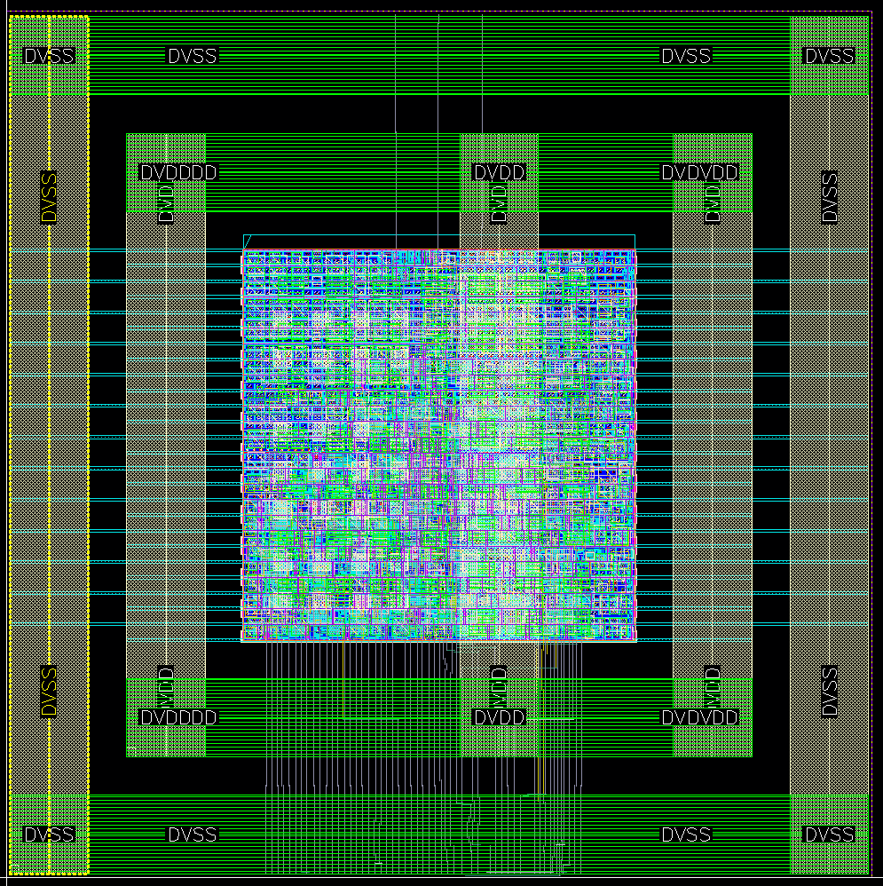
Fig. 8: SPI Auto place-n-route layout
The second one is the SPI module. It is 100 * 100 micrometers. The thin gray wires at the bottom are used to get the outputs from the decoder, and the three wires at the top are SPI signals.