
PCB DESIGN
The PCB board was designed in KiCad 7.0. It supports a surfboard/solderboard such that our IC can be mounted/soldered on these boards and the board headers can be plugged into the header sockets on PCB. The PCB is designed to allow mount of microcontroller board directly onto the PCB. The PCB includes the power supplies, level translators, clock generators, voltage references, current bias, and crystal filter, making the required external connection being only a single USB to micro-USB cable. The following is the overall schematic:
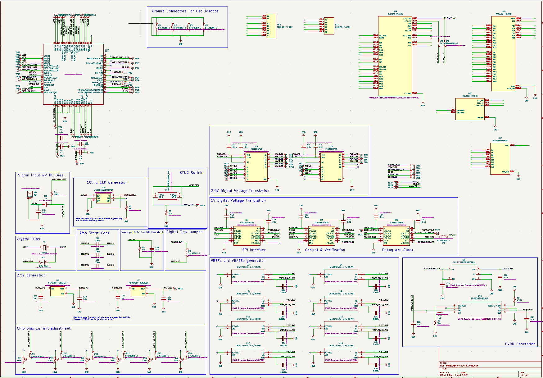
Fig. 1: PCB schematic
The general powering strategy is to get both analog and digital power from the microcontroller power supplies. The 2.5V AVDD analog power supply is generated from an 2.5V LDO that takes in the 3.3V supply on the STM32 nucleo board. The 5.0V supply on the nucleo board is first converted down to about 1.8V using a buck converter, then regulated with a 1.0V LDO, which is used as 1.0V DVDD digital power supply. The voltage references use 2.5V VREF that is generated from another 2.5V that also takes in the 3.3V supply on the nucleo board.
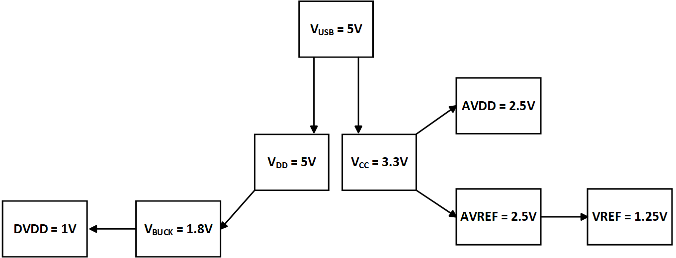
Fig. 2: Power supply block diagram
The clock used for the decoding logic is generated with a programmable oscillator that is fixed at 10kHz. The LNA input is DC biased with a resistor from VREF_LNA_1V25, and AC coupled via a 1nF ceramic capacitor to the antenna output. All of the digital signal (SPI, control signals, debug/clock signals) are level shifted using some bi-directional level shifter ICs that bridges between 1V and 3.3V. All of the AGC control bits are also level shifted using similar level shifter ICs that converts between 2.5V and 3.3V, as AGC bits are acted on 2.5V device transmission gates.
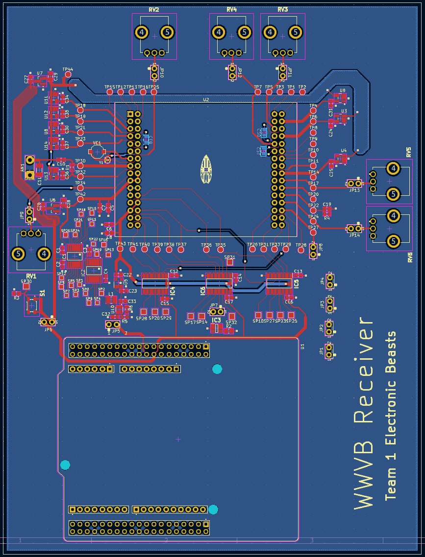
Fig. 3: PCB layout overview
The NUCLEO-F446RE microcontroller board pinout is the following:
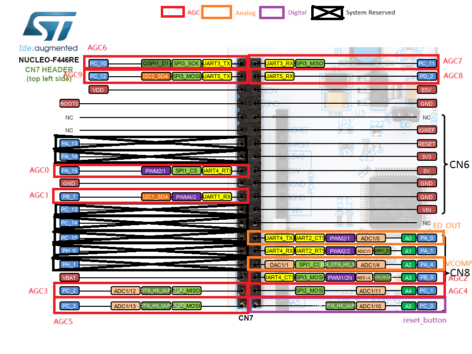
Fig. 4: Board left side pinout
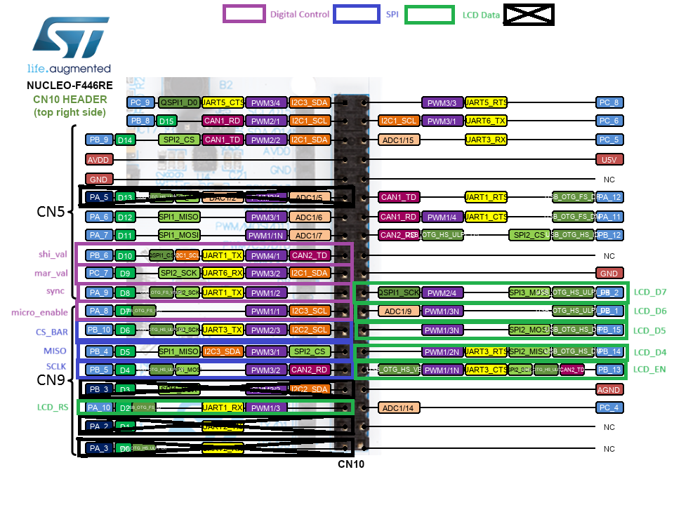
Fig. 5: Board right side pinout
The final PCB assembly view:
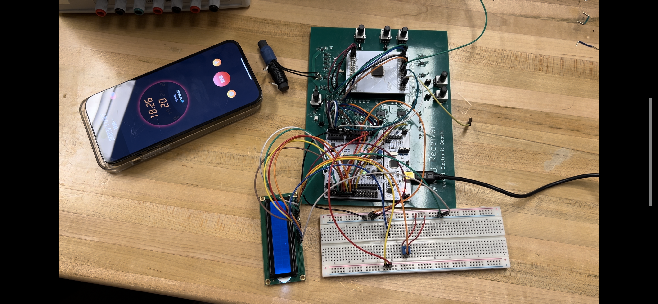
Fig. 6: Final board assembly view