
MEASUREMENT RESULTS
FERRITE ROD ANTENNA
The tuned antenna characteristic was measured using frequency response analysis tool on the oscilloscope. By winding some turns of wires around the ferrite rod. The signal was sent through this new wire and magnetically coupled to its output. The transfer function of the antenna was measured:
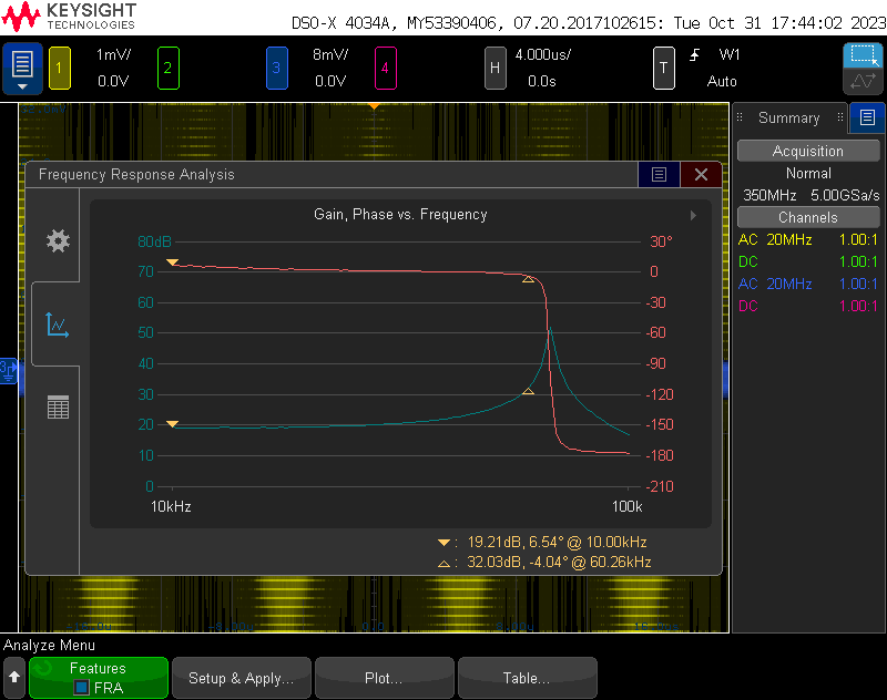
Fig. 1: Ferrite rod antenna transfer function with 1.6pF tuning cap
The center frequency of the antenna is at 67.61kHz. The quality factor of the antenna is 52.3.
LOW NOISE AMPLIFIER
The LNA transfer function was also measured:
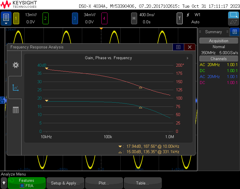

Fig. 2 & Fig. 3: LNA transfer functions with respect to the either side of the differential output
The gain of the amplifier is 17.9dB (single-ended). The bandwidth of the amplifier is 331.1kHz.
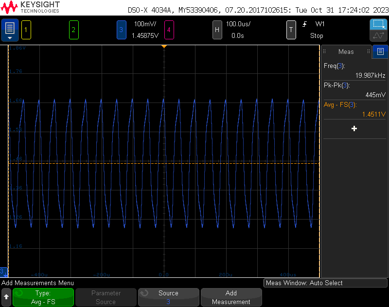
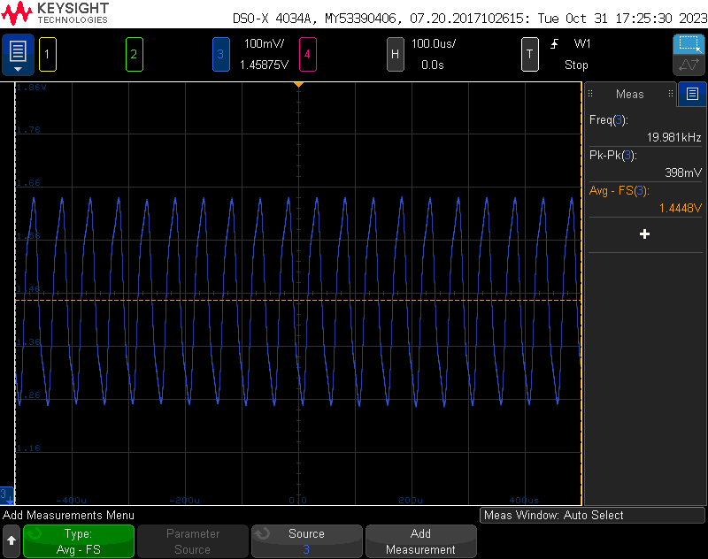
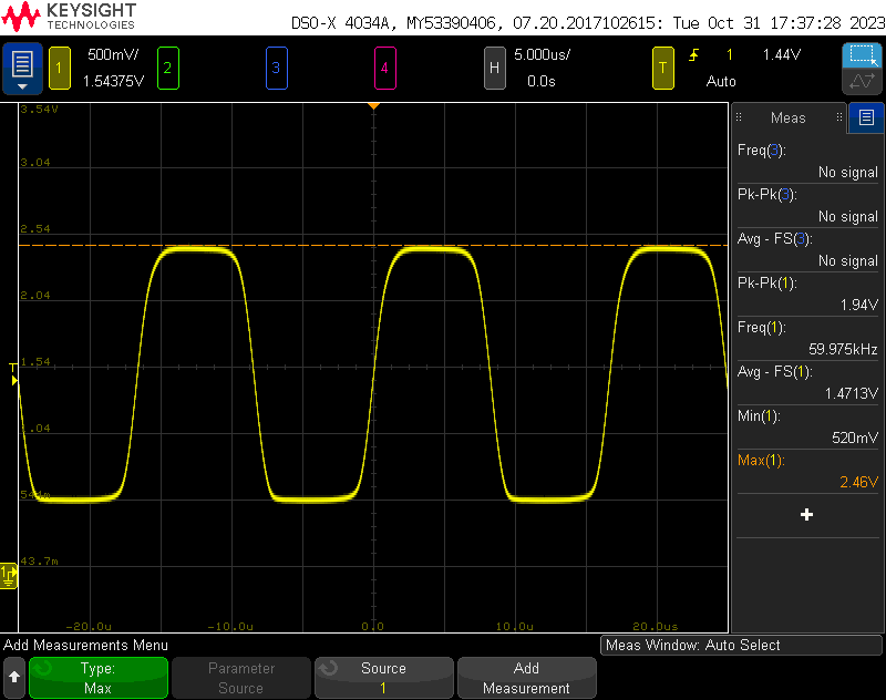
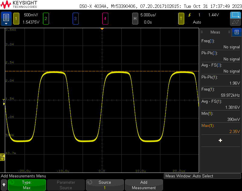
Fig. 4 ~ 7: LNA output pair transient (4 & 5) and full swing measurements (6 & 7)
The output DC operating point for QOUT node is 1.451V, and for VARCAPOUT node is 1.449V. The output swing for QOUT node ranges from 0.52V to 2.46V, and for VARCAPOUT node ranges from 0.39V to 2.35V.
CRYSTAL FILTER
Fig. 8: Recorded data points of crystal filter
The gain of the transfer function is measured from the LNA input to the crystal filter output. This part of measurement was done by manually tuning function generator output frequency. The center frequency of the crystal filter is at 59.996kHz, and the measured quality factor is extremely high: 46872. The gain at 60kHz is 8dB less than the center frequency.
BUFFER AMPLIFIER
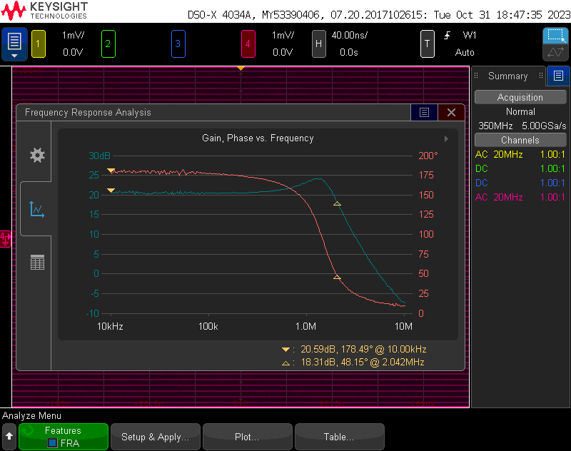
Fig. 9: Buffer amplifier transfer function
The gain of the buffer amplifier is 20.59dB, and the bandwidth is 2.042MHz.
PROGRAMMABLE GAIN AMPLIFIER
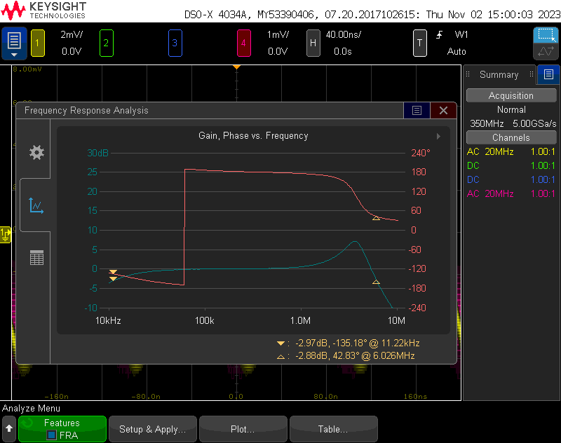
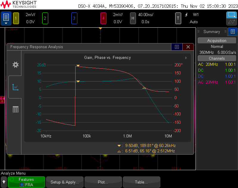
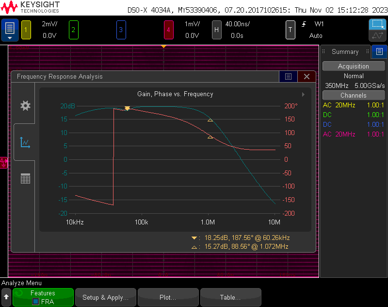
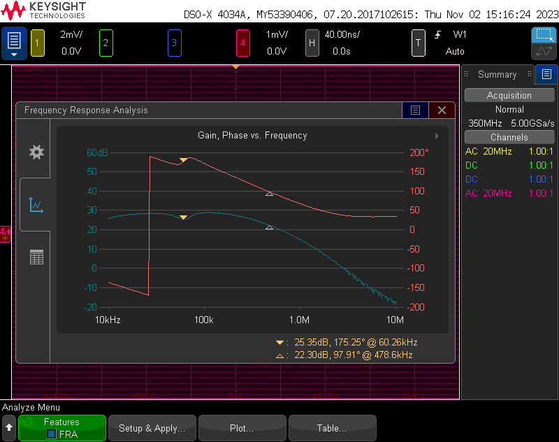
Fig. 10 ~ 13: Transfer function from PGA input through first cascade stage with 0/1/2/3 10dB gain steps
Side note: The transfer function of 4 10dB gain steps is ignored. The 4th gain step was working properly during our initial testing phases, but suddenly stopped working for unknown reason. The measured gain under different setting is: -0.5dB, 9.5dB, 18.25dB, 25.35dB. The bandwidth reduces from 6.026MHz to 478.6kHz.
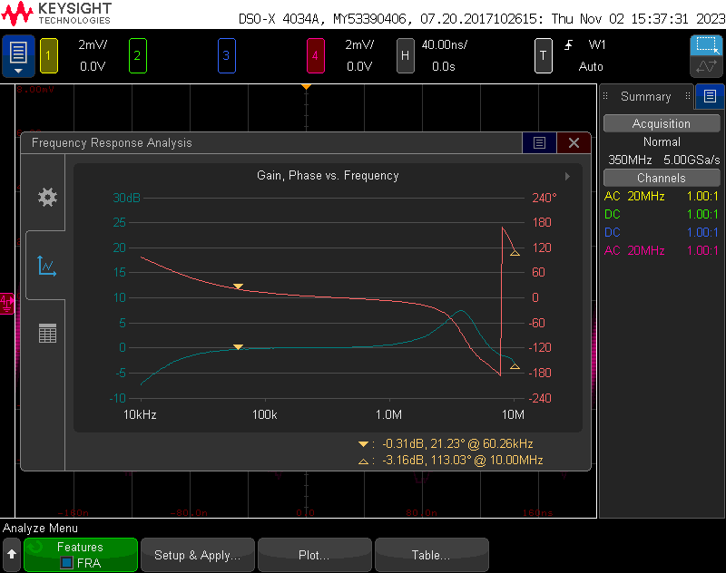
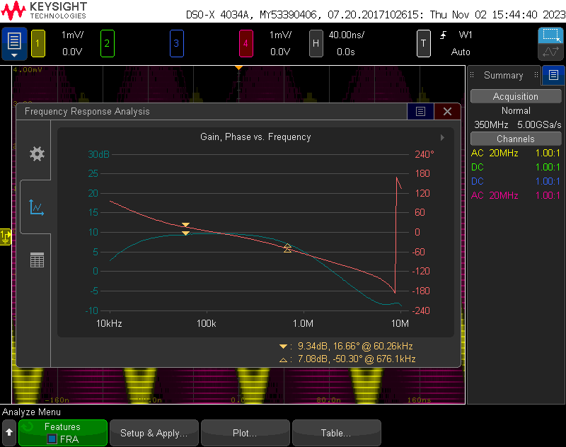
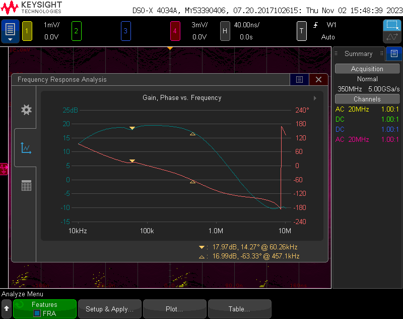
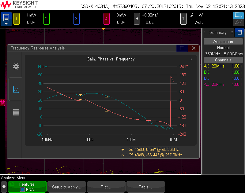
Fig. 14 ~ 17: Transfer function from PGA input through second cascade stage with 0/1/2/3 10dB gain steps when first stage has 0dB gain
The measured gain under different setting is: -0.31dB, 9.34dB, 17.97dB, 25.15dB. The bandwidth reduces from 10MHz to 257kHz.
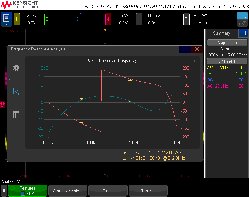
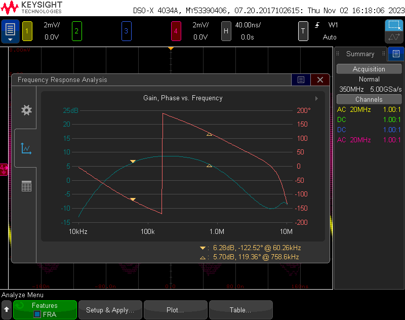
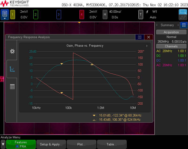
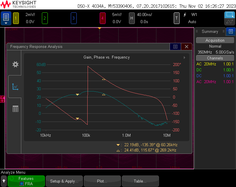
Fig. 18 ~ 21: Transfer function from PGA input through third cascade stage with 0/1/2/3 10dB gain steps when first and second stage have 0dB gain
The measured gain under different setting is: -3.63dB, 6.28dB, 15.01dB, 22.19dB. The bandwidth reduces from 812.8kHz to 269.2kHz. The reason for the reduce gain may come from the high-pass AC-coupling capacitors through the cascading stages.
ENVELOPE DETECTOR
Fig. 22: Envelope detector output stable voltage vs. input peak voltage of the sinusoid
Because of the large RC constant, a rough transfer function between input amplitude to output voltage can be determined by measuring the envelope above a 60kHz sinusoidal input, even though the relationship between input and output is non-linear. The envelope detector output cannot reach the supply voltage, maximum at 1.769V.
THRESHOLD DETECTOR
Fig. 23: Threshold detector output voltage vs input voltage with hysteresis sweep
The schmitt trigger was tested under VCOMP = 1.29V. The low-to-high point is 1.307V, and the high-to-low point is 1.267V.
MICRO_ENABLE SIGNAL
Fig. 24: Micro_enable signal oscilloscope probing result
This image shows that after the reception is done (this is shown on the phone where a full minute has ended), the micro_enable is pulled high by the chip. This is used to notify the off-chip microcontroller that the data is ready to be fetched.
SPI WAVEFORM
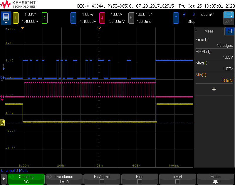
Fig. 25: Example SPI output waveform probed and shown on oscilloscope
This is a complete run result after sending a test signal into the antenna. The signal in blue is the serial output data. The signal in magneta is the SPI clock. The signal in yellow is the SPI chip select, which is an active-low signal. The data is sent out in completely reverse, i.e. DST[0] will be sent first and min_40 bit will be sent last. Please refer back to "System Overview" page for signal format. In this test case we are using the same test case provided in the Enhanced WWVB Broadcast Format (Page 12). The implemented SPI has idle clock at logic '0', has valid data at the positive edges of the clock, and shifts out new bit at negative edges of the clock. The decoded 53 bits are:
110100100 100000010 101000110 000101000 111001000 00000110
which matches the reverse order of the one-minute test case.
VALIDATION BITS
Fig. 25: Marker validation and shifting validation bits shown on oscilloscope
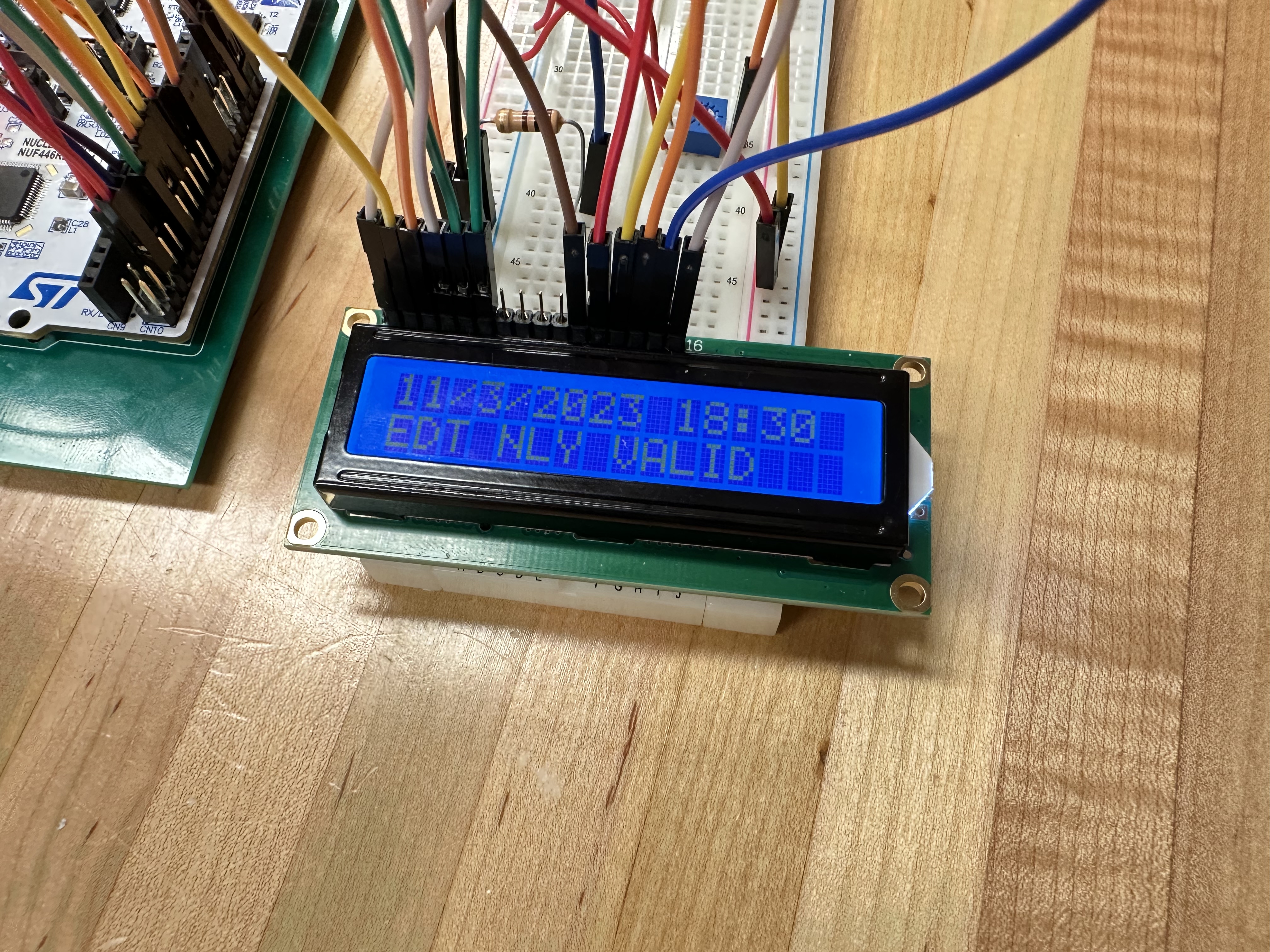
Fig. 26: Validation result on real signal run test
Both validation bits will be pulled high if there is no error in number of markers and the position of markers. If either one check fails, the corresponding check will be pulled low, and the off-chip microcontroller will show "INVALID" on the LCD screen.