
PCB Design
In order to create a functioning product, we need to integrate digital clock IC with the PCB. The PCB provides external support for the IC chip. It includes:
- 2 different power supplies: a 9V battery and a 2.0 USB connection
- Push-button switches for reset and setting mode
- Crystal reasoning at 32.768kHz
- External Crystal Oscillator
- Six 7-Segment LED Displays
- Slide switches for selection of power, clock selection, external clock selection, mode selection
The biggest challenge was operating the LED displays at 1.8V. Since our power supply is 1.2V we had to use level shifters and one more voltage regulator. Operation with the 9V battery and the signal from the internal oscillator is a standalone operation. We designed the PCB using.Diptrace Software. The dimension of the board is 9.35 x 7.26 cm, about the size of a small book.
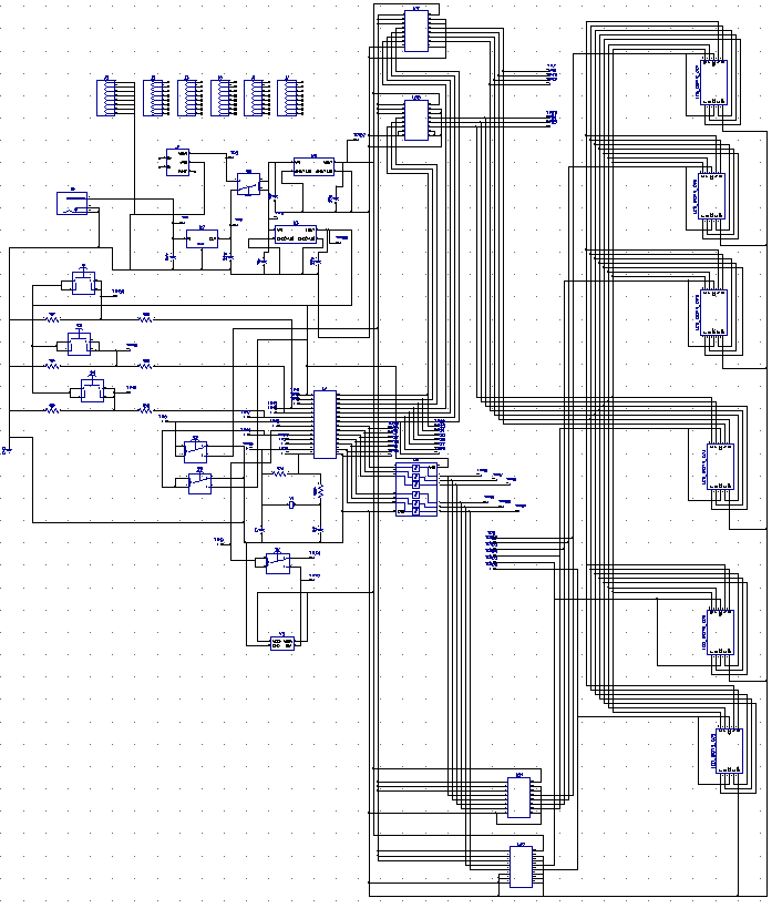
Fig. 23: PCB Schematic
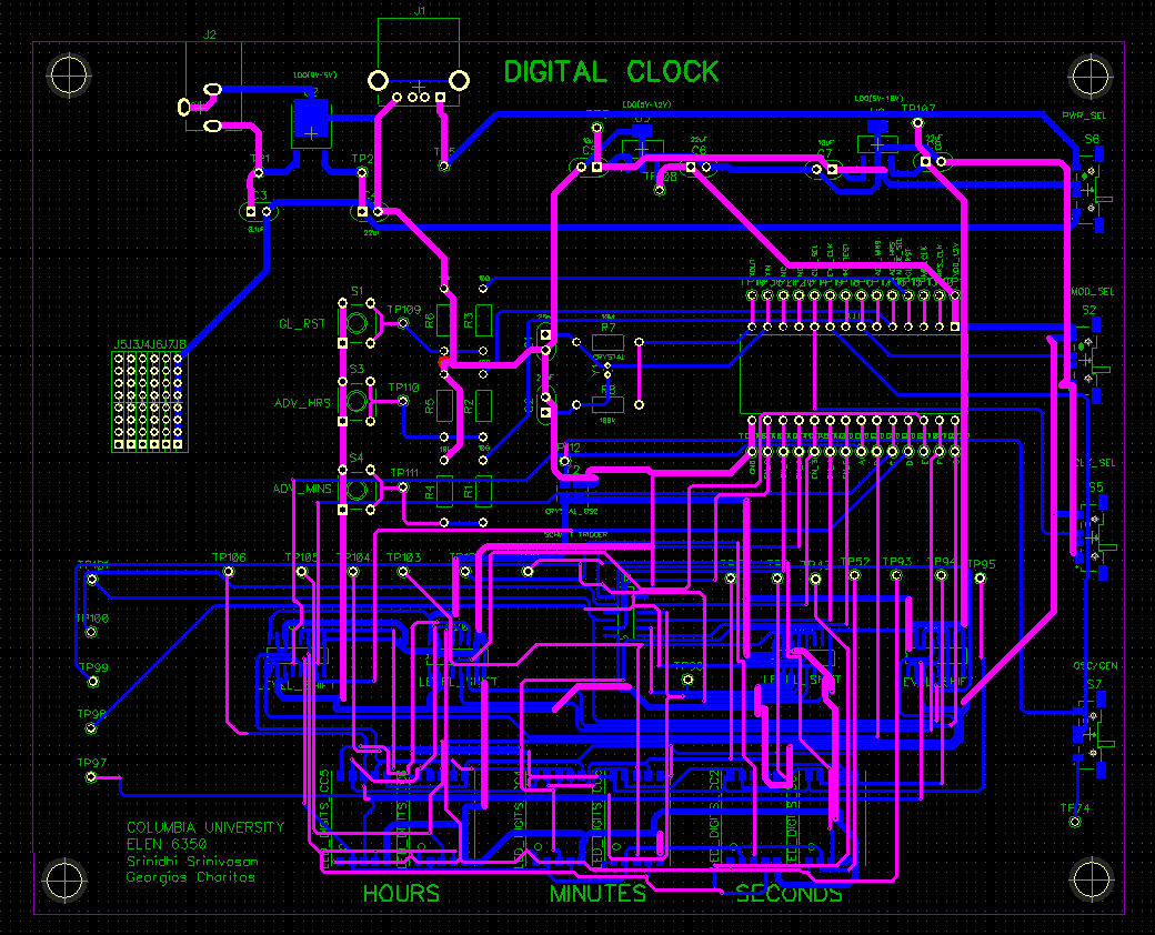
Fig. 24: PCB Layout
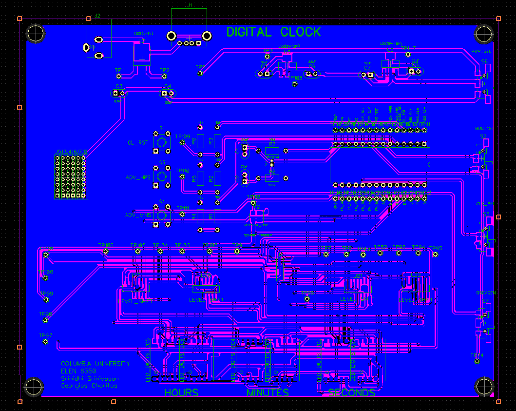
Fig. 25: PCB Layout with copper pour
Power Circuitry
The PCB has two different power sources, a portable 9V battery through the jack connector and a 5V 2.0 USB connector. This way it can operate both standalone and plugged to an external power source. The 9V battery also has a 9 - 5V voltage regulator. After the source is selected via a slide switch, we include a 5 - 1.2V voltage regulator for the Vdd and a 5 - 1.8V voltage regulator for the level shifters. Decoupling capacitances are placed appropriately.
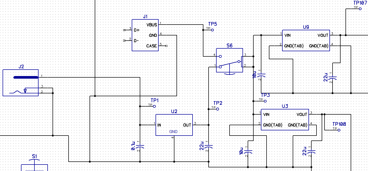
Fig. 26: Power Circuitry
IC PIN Connection
The core component of this project is the IC pin that MOSIS manufactured with a DIP-28 pin package. We added a test-point next to every pin to aid the testing process.
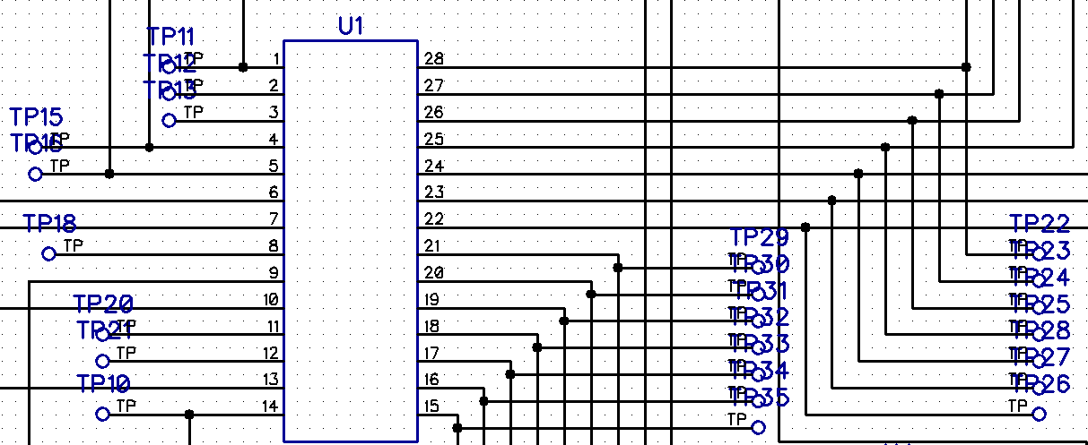
Fig. 27: Pin connectivity
| Pin# | Pin Name | Pin# | Pin Name |
|---|---|---|---|
| 1 | VDD | 15 | GND |
| 2 | HRS_CLK | 16 | EN_0 |
| 3 | MIN_CLK | 17 | EN_1 |
| 4 | GL_RES | 18 | EN_2 |
| 5 | ADV_HRS | 19 | EN_3 |
| 6 | ADV_MIN | 20 | EN_4 |
| 7 | MODE_SEL | 21 | EN_5 |
| 8 | 1Hz_TEST | 22 | A |
| 9 | EXT_CLK | 23 | B |
| 10 | CLK_SEL | 24 | C |
| 11 | NC | 25 | D |
| 12 | NC | 26 | E |
| 13 | XIN | 27 | F |
| 14 | XOUT | 28 | G |
Table 1: Pin Configuration
Push-Button & Slide Switches
The push-button and slide switch circuitry is shown below. Normally closed configuration is utilised for push-buttons.
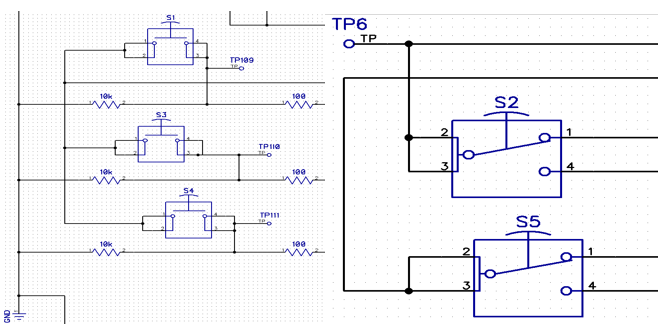
Fig. 28: Push-button & Slide switches
Oscillator Circuit
On the board we have placed two oscillating sources. A crystal which is connected to the internal chip oscillator and an external crystal oscillator just in case our crystal was not working properly. Both resonate at 32.768kHz. The external one is connected to a shunt switch that chooses between that one and the external frequency generator.

Fig. 29: Crystal & External Crystal Oscillator
7-Segment LED Display circuitry
The LED circuitry was the most challenging part of the PCB. We have 7 segment display signals A-G and 6 enable signals EN0-EN5.
- 7-Segments
- Enable Signals
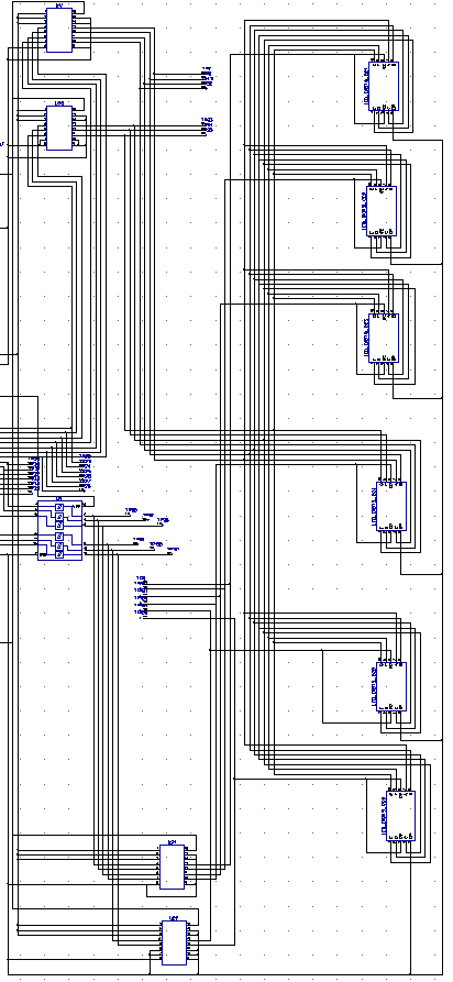
Fig. 30: PCB LED circuitry
After verifying schematic & layout of the PCB we generated the gerber files and sent them to PCB minions. Below we also provide a 3D model of the PCB along with its components.
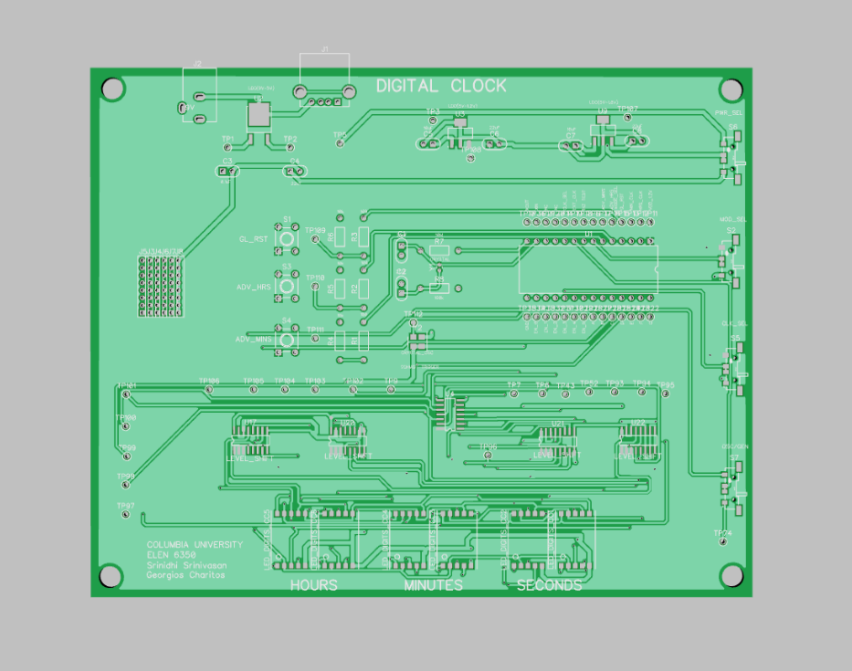
Fig. 31: PCB Product
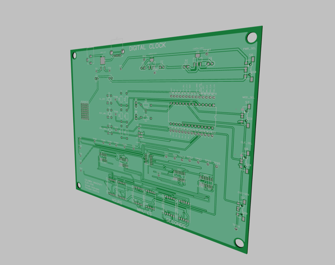
Fig. 32: PCB Product
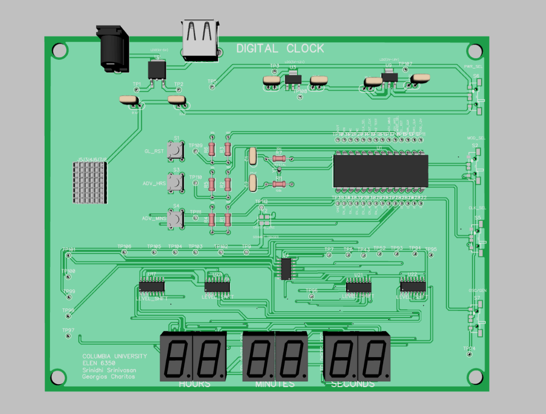
Fig. 33: PCB Product with components
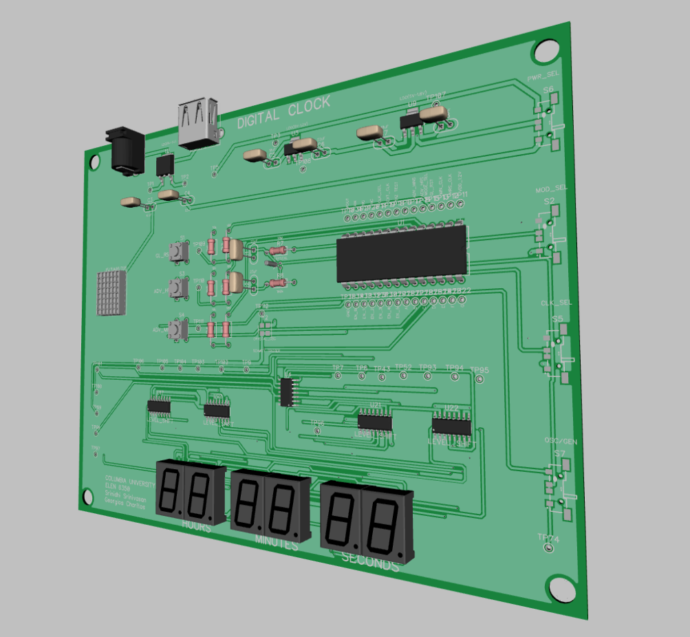
Fig. 34: PCB Product with components