
Block Description
The entire IC is composed of the following blocks.
Crystal Oscillator
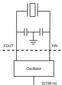
Fig. 3: Crystal Oscillator Circuit
- Off chip crystal
- On-chip Oscillator
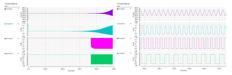
Fig. 4: Crystal Oscillator Simulations
Clock Select Stage
The clock select stage is a 2x1 multiplexer that selects between the 32.768kHz signal from the crystal oscillator and the 32.768kHz signal from an external frequency generator.
Frequency divider chain
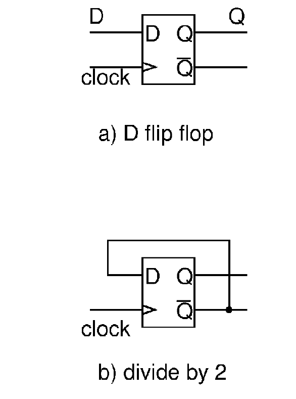
Fig. 5: Division by 2
The frequency divider is a chain of 15 D-Flip-Flops with reset. Each stage is configured so as to produce a division by 2 in the signal frequency. The chain has 2 outputs:
- One after the second stage to produce 8kHz frequency for the Multiplexed display driver
- Another after 15 stages for the 1Hz frequency to be fed to the seconds counter
Seconds, Minutes, Hours Counter & Setting Mode
The seconds & minutes counter include a modulo 10 counter and a modulo 6 counter each. These counters are resettable and they count from 0-9 and 0-5 respectively. Between them there is a 2x1 multiplexer that selects between normal mode for the minutes and setting mode for the minutes. The hours counter include a modulo 10 counter and a modulo 3 counter. These counters are resettable and they count from 0-9 and 0-2 respectively. Between the minutes and hours counter there is also a 2x1 multiplexer that selects between normal mode for the minutes and setting mode for the hours.
Display Section
The display section consists of four components:
- Multiplexed Display Driver
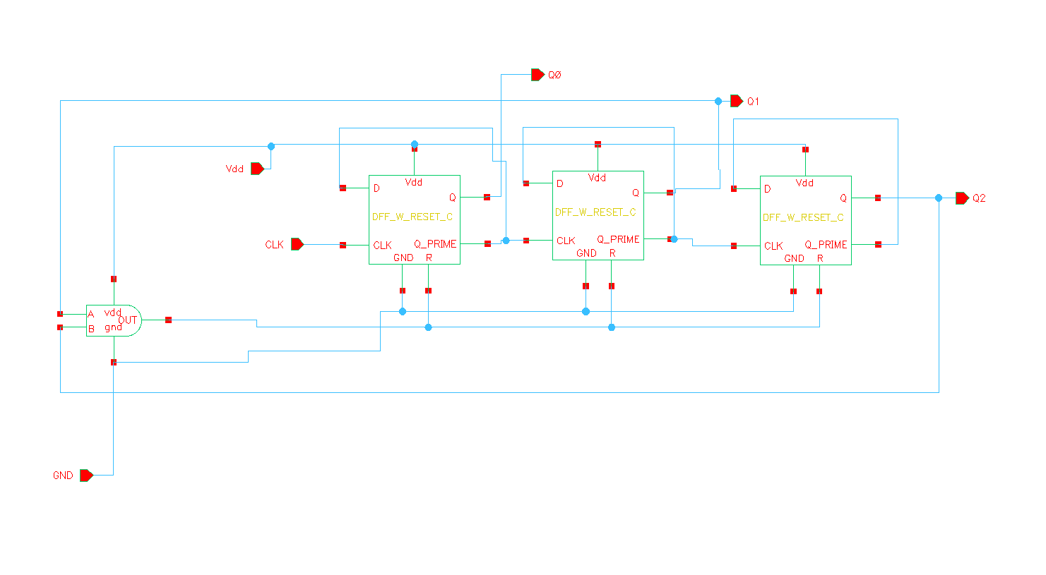
Fig. 6: Modulo 6 counter
- Four 6x1 multiplexers

Fig. 7: Multiplexed Display Circuitry
- 4-7 Decoder
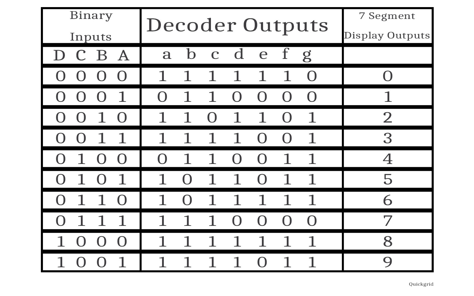
Fig. 8: 7-segment decoding truth table
- 3-6 Decoder
Interface
The chip communicates with the outer world using a DIP-28 pin package. The input pins are the Vdd and gnd, the 2 setting mode pins, the global reset, the oscillator input, the mode selection and the clock selection. The rest are output pins like the 6 enable signal, the 7 segment pins, the oscillator output and the hrs and mins frequencies and the 1Hz test pin which is bidirectional.