
Conclusion
As far as the chip function is concerned, the chip operated correctly and the PCB design was on target as well as the Integration. Thus, the product result was successful. In terms of power consumption, our chip has a 1.2V power supply and consumes very small amount of power. The most power consuming section is the LED circuitry of the PCB.
Concerning future work, we could have extended the chip's function by adding AM/PM display and an alarm function.
The digital clock project and the vlsi design lab course in general, offered us a wide variety of knowledge. The most important as mentioned in the introduction is the fact that we obtained hands-on experience through the entire IC design flow all the way from deciding system-level specifications to testing the final tape-out chip on a PCB.
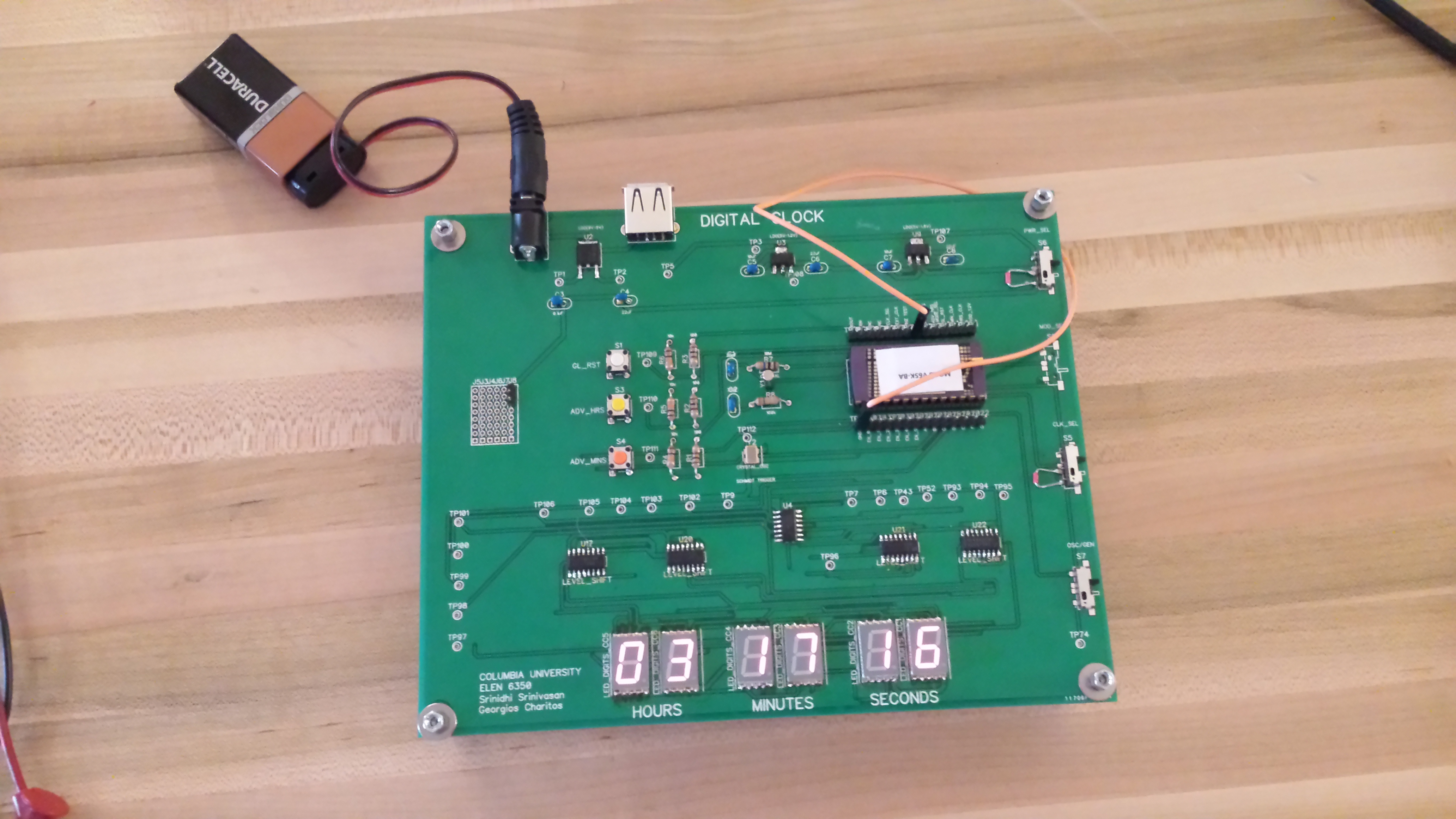
Fig. 41: Final Digital Clock