Testing
DC Testing
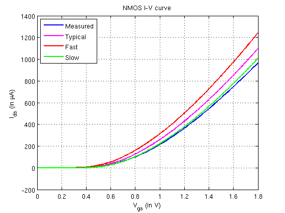
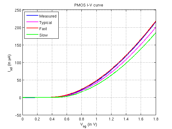
The IC was received on a Dual In-line 28 pin package (DIP28). It was assembled on a fabricated PCB and tested. To determine agreement between simulation and measurements in silicon, as a first step, the process corner of the fabricated chip was determined by running I-V sweeps on diode connected PMOS and NMOS test structures on the chip. The results are displayed in FIG 1. The NMOS is in the slow corner and the PMOS is in the fast corner.
AC testing
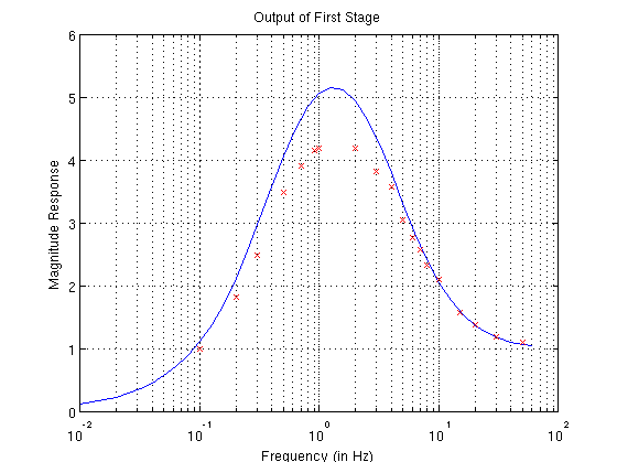
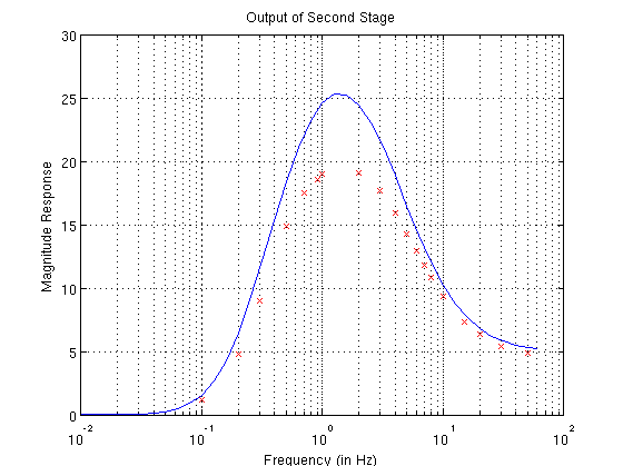
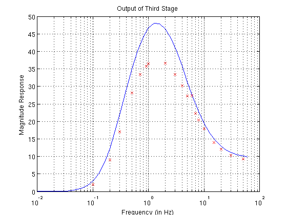
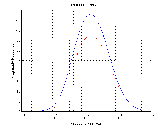
The AC response of the Heart rate filter chain was characterized by introducing a sine wave at the input of the filter chain and looking at the response at the output of each of the stages.This was plotted against simulation to test agreement. There appears to be a mismatch, (possibly on account of component variations), in the first stage which propogates through all four stages. The results are in FIG 2.
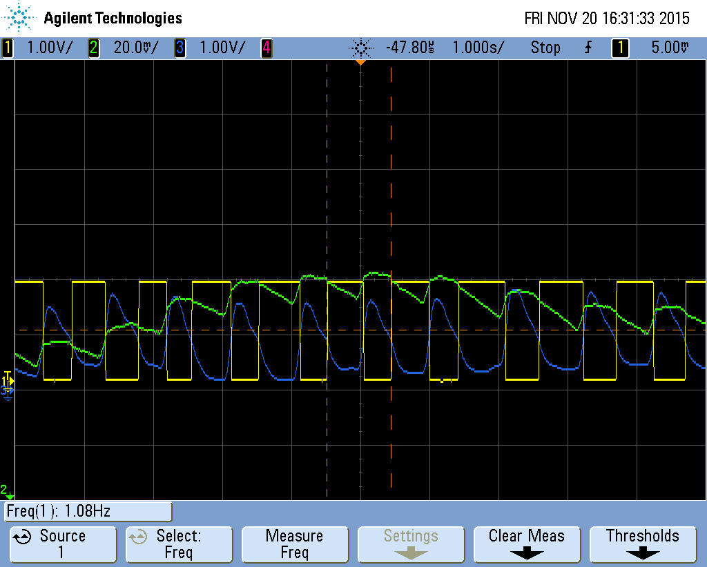
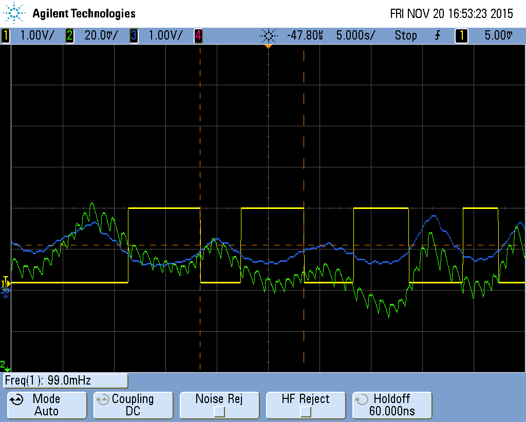
Tests with the PPG sensor
The chip was then tested with the signal from the PPG sensor. The output of the sensor, the output of the heart rate filter chain and the output of the comparator are plotted in FIG 3. The corresponding signals for the respiratory rate filter chain are plotted in FIG 4.