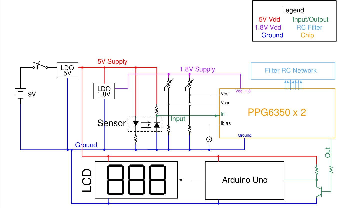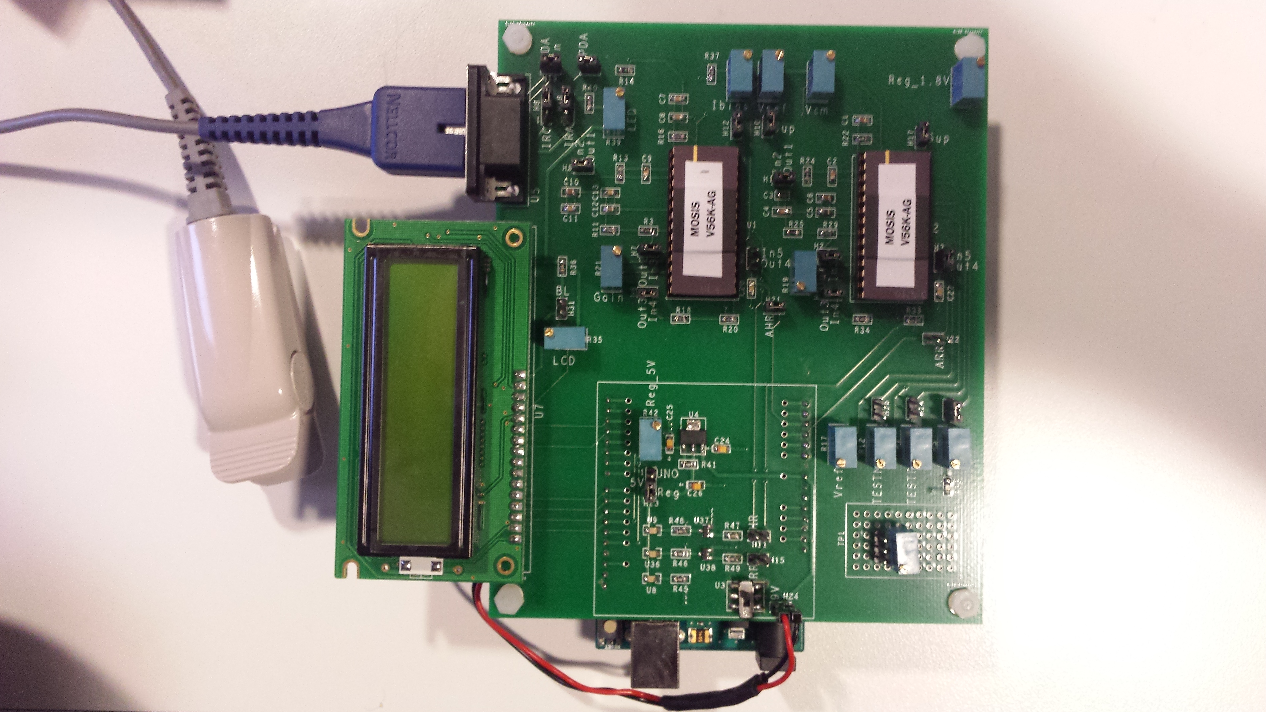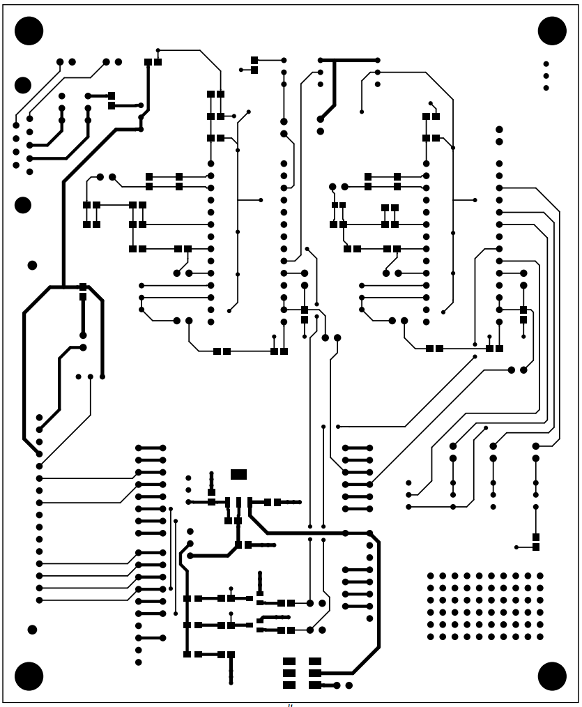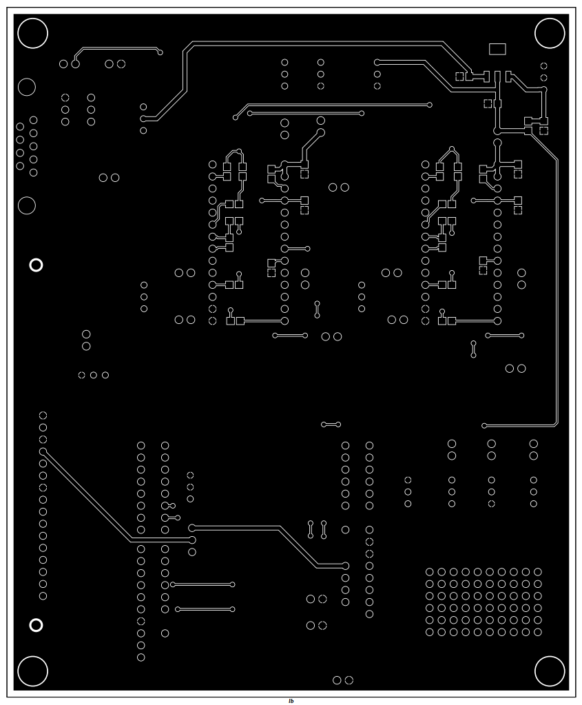
PCB Design
A board was designed using Cadence Allegro to test the performance of the IC. The board performs the following functions -
- Provided an easy way to interface the sensor to the IC using a DB9 socket.
- Allow the insertion of a multitude of resistors and capacitors, which in conjunction with the IC, realize the filters and amplifiers necessary for estimating the Heart rate and Respiratory rate.
- Provide a socket for interfacing with a microcontroller (Arduino Uno), to perform digital processing on the filtered snd amplified signal waveform.
- Level shift the 1.8V logic of the IC to drive the 5V logic of the Arduino.
- Provide a way to mount an LCD screen for displaying the result.
- House the power regulation unit to generate stable 5V and 1.8V supplies to power each of the above blocks.