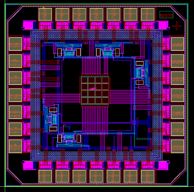
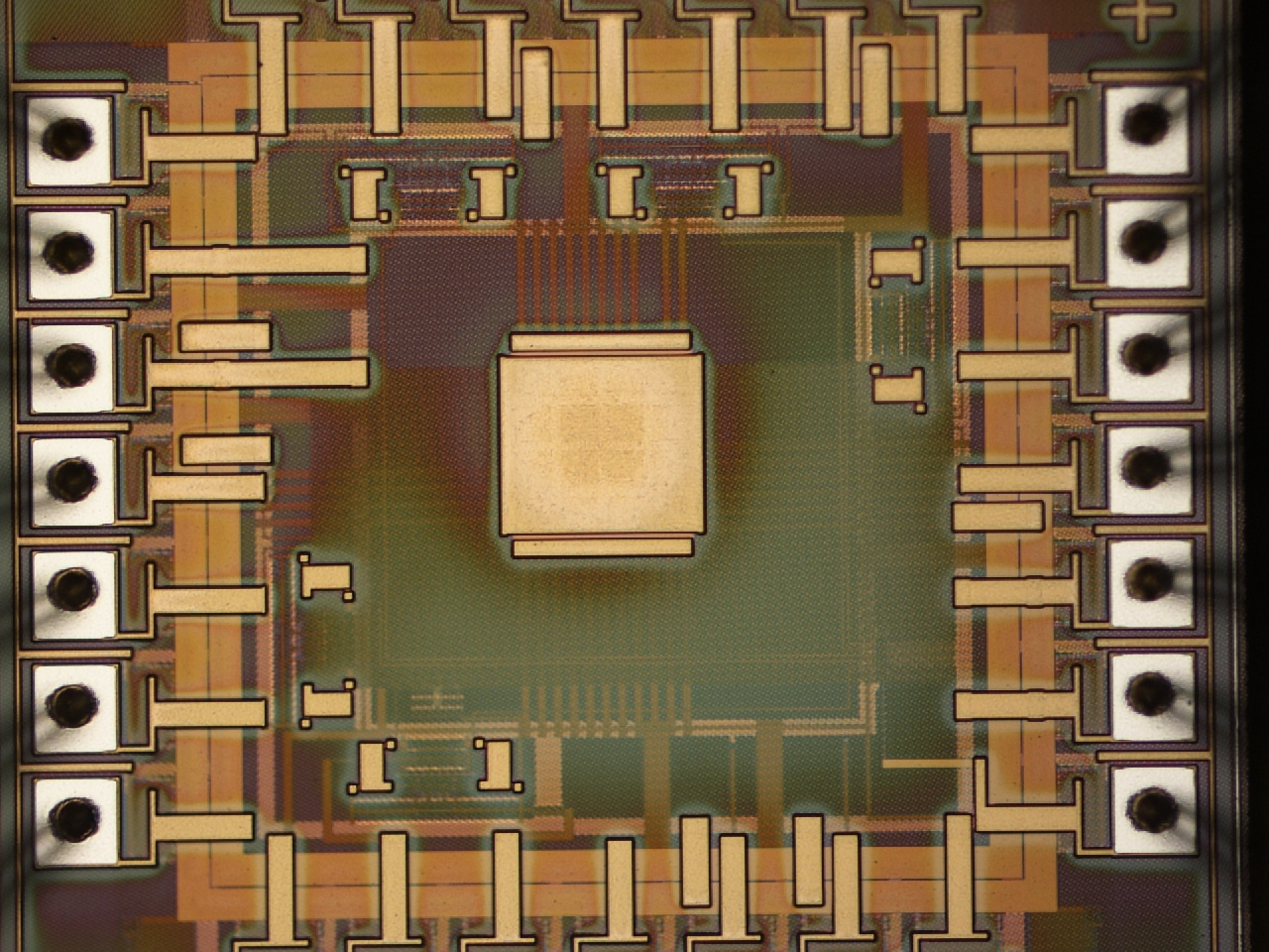
Top Level Layout
The IC is comprised of 5 Operational Transconductance Amplifiers (OTAs), one of which is configured as a comparator with hysteresis. The OTAs have similar layouts and are repeated for all the instances. The Vdd and Vss lines are configured as rings and the operational amplifiers are nested in between the Vdd and Vss rings.
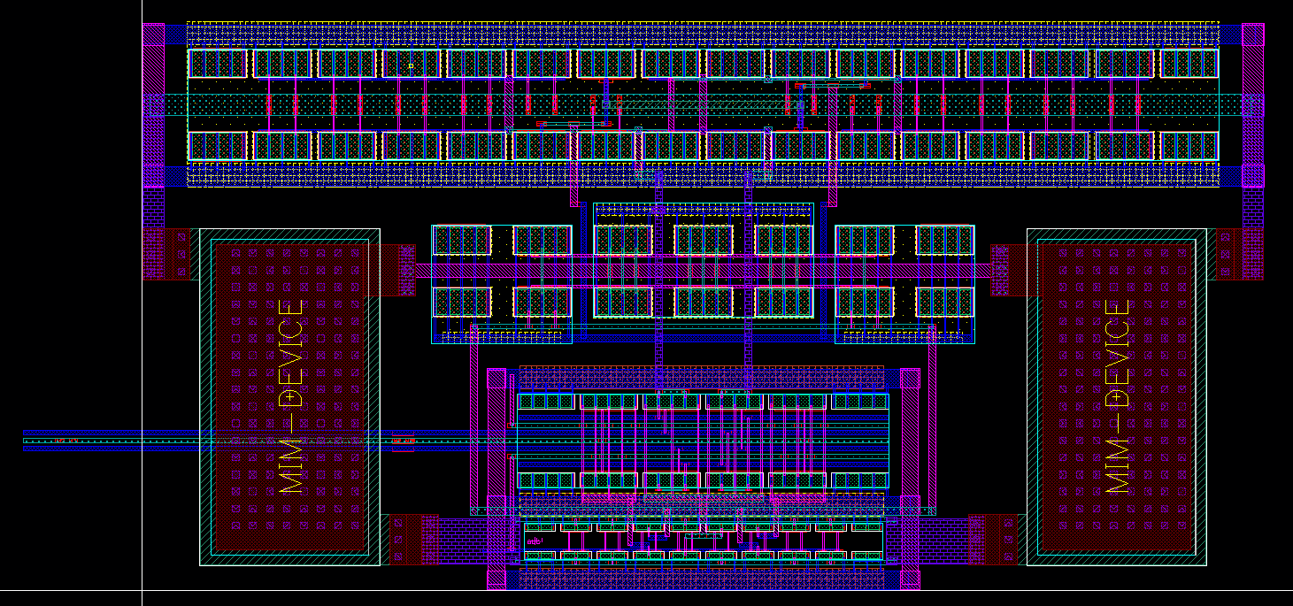
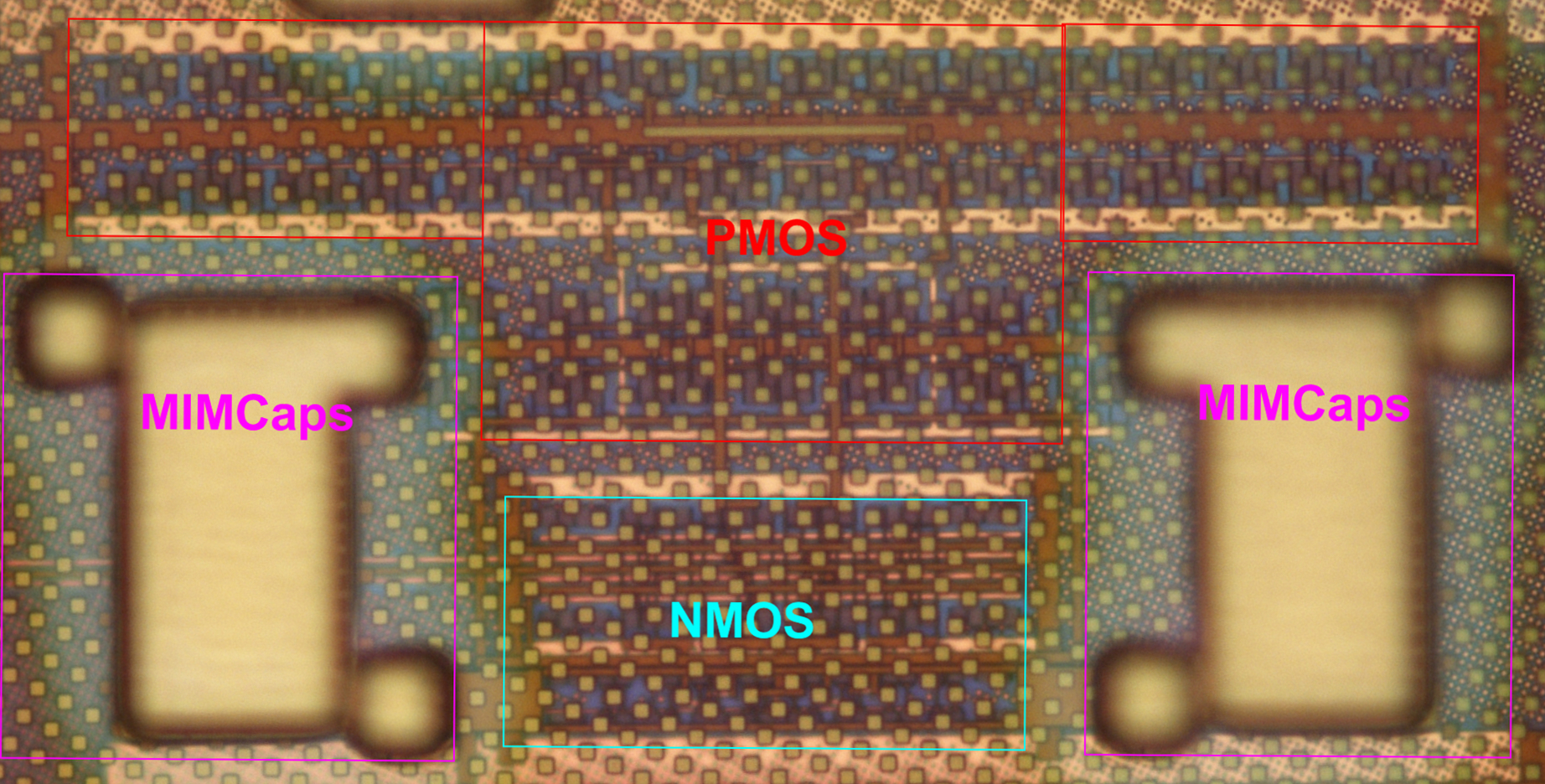
OTA Layout
Each OTA has been laid out in a completely symmetric manner, the differential NMOS transistors and the PMOS transistors have been laid out in a common centroid fashion with the PMOS and NMOS transistors corresponding to different stages being interleaved to guard against systematic offsets. The Miller capacitor has been implemented using a Metal-Insulator-Metal (MIM) capacitor and has been split into two parallel components to preserve the symmetry of the layout. The Vdd and Vss lines have been laid out horizontally at the top, and bottom respectively along the width of the OTA to ensure easy access to the supply and good substrate/well connectivity. Dummy MOSFETs were implemented for the PMOS and the NMOS to ensure that the physical environments around the PMOS and NMOS were similar.
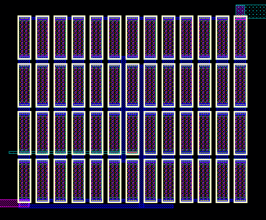
Resistor Bank layout
The ratio of feedback resistors around the OTA in the hysterisis comparator dictate the amount of voltage hstersis in the comparator. Well matched layout ensures that the implementation in Silicon matches the designed value. The Resistors were laid out in a common centroid fashion with the ratio of resistors being dependent only on the ratio of the number of segments. The Resistor R1 is nested within the Resistor aR1 to improve matching and reduce the effects of systematic offsets.The larger resistor acts as a dummy for the smaller one. There was however, no dummy ring implemented for the larger resistor.