Testing
PWM modulation is critical for correct operation of class-D amplifier.Triangular wave generator is essential for the correct PWM modulation operation. The triangular wave we designed is 1.2V peak to peak at 750 KHz. Figure 1 shows the plot of the triangle wave being generated. It has 1.2V peak to peak voltage, but with 630 KHz frequency. The frequency mismatch is expected since the resistor and capacitor on chip suffers about 20% variation respectively.
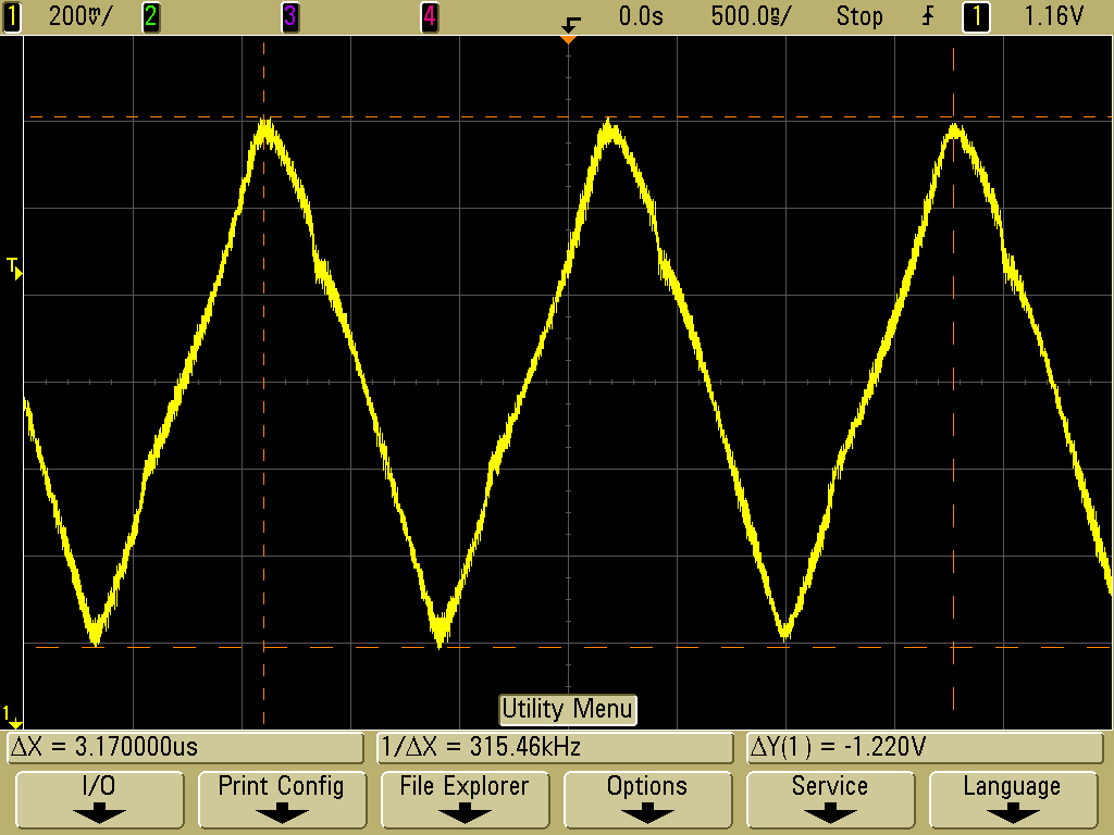
Figure 2 shows the comparator output with no input apply to the chip, and Figure 3 shows the differential output of the chip in the case. It is expected to have 50% duty cycle for all these signals.
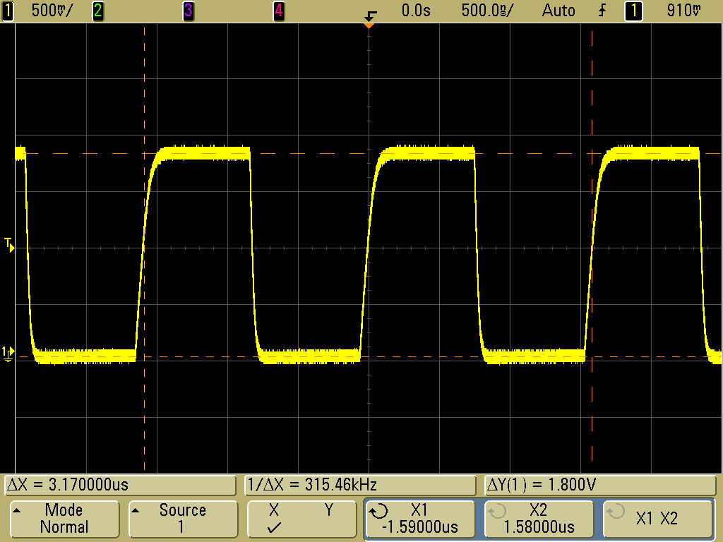
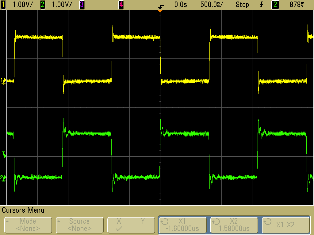
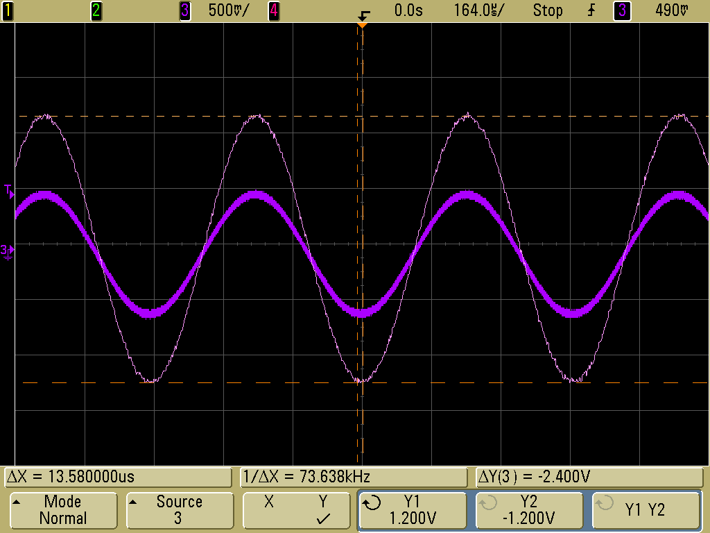
Figure 4 shows the differential output after the off chip low pass filter with gain of 2. The gain can be adjusted by changing the ratio of the feedback resistor.
Efficiency Measurements
The efficiency is defined as \[ \eta = \dfrac{P_{Load}}{P_{supply}} \] For class-D amplifier, the major loss in efficiency is assumed due to the voltage division between the output mosfet and the load. So the efficiency measurements can be simplified to \[ \eta = (\dfrac{V_{Load}}{V_{supply}})^2 \] Figure 5 shows the efficiency across the frequency.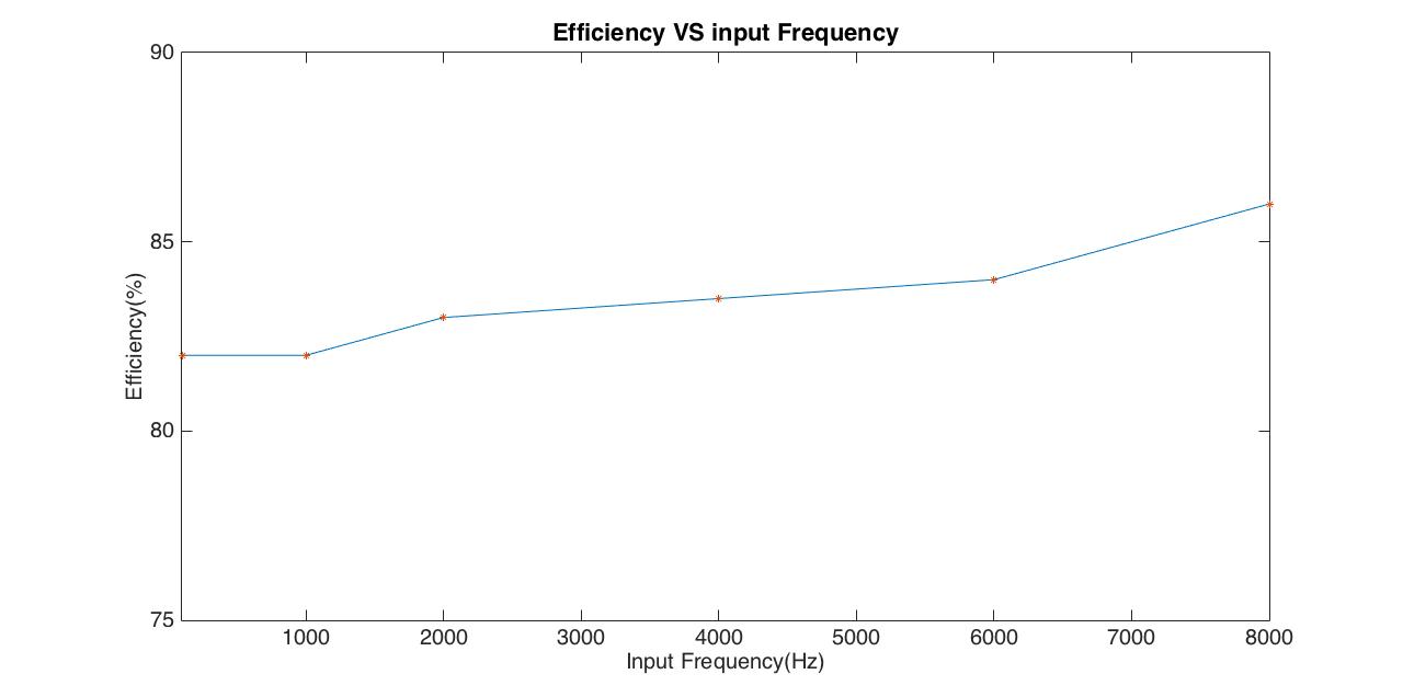
Distortion Measurements
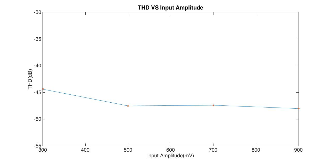
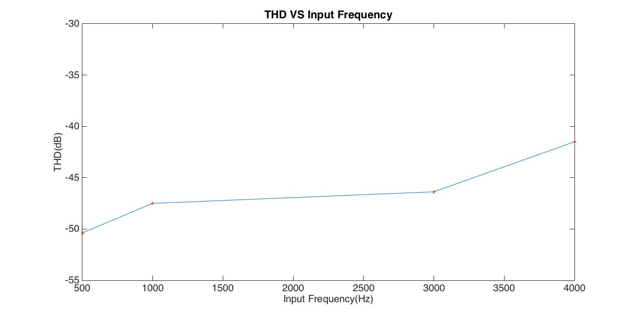
The total harmonic distortion is defined as \[ THD = \dfrac{\sqrt[2]{(V_2^2+V_3^2+ \ldots)}}{V_1^2} \] Where $V_1$ represents the amplitude at fundamental frequency, and $V_n$ represents the amplitude at harmonics. Figure 6 shows the THD at 1 KHz with various peak to peak input, and Figure 7 shows the THD for different frequency with 700 mV peak to peak input.